I am curious to learn the optimal value for the I2S resistors.
2 or 3 reversed signal diodes in serie on each I2S line like John lately made (with him latest tda1541 researchs).... but I will be curious if a 100 ohms resistor (the same as RyanJ uses for the 6k8 R or some smt Vishays or Sussumu low noise could be heared as well ?)
A lot of informations on the "Grounding TDA1541" thread as well !
Hi Ryan
Perhaps you should start with a series resistor to the I2S lines first.
Also you might try a 1uh inductor between the salas reg & the input caps.
If there's improvement then change the input cap to say an Elna Silmic
Cheers
Hi Jaffrie,
Interesting reading about tank circuits and how they operate, does adding the 1uh inductor increase output impedance of the shunt reg? So if this inductor "tunes" the power supply to operate at its resonant frequency, is there any danger of oscillations?
Ryan,
I re read all the thread about "grounding the tda1541" here on Diya and spent a very good moment like at the crazy time we brainstormed to make all together the Distinction1541 one year ago (anniversarry cake please 🙂 )!
I must apologize no to suceed to involve more experienced people which are present on diyaudio, nevertheless still thinking the Distinction is the best ever made diy TDA1541 core board produced for more than one people 🙂
I read more about the ground (and the complex three voltage rails of the 1541) and understand now why my proposals above are sheety !
Yeah, its amazing how much information is on this forum if you dig deep into the past, a great resource.
Ah, when not using simultaneous mode on the Distinction1541 :
Better to shunt the pin 4 to the Gnd with a strap on the vias made for the clock or lets the pin 4 float ?
From my experience it still works if you float it but its best if you tie it to gnd.
I am curious to learn the optimal value for the I2S resistors.
But the use of 22-100 ohms resistors in the I2S lines applied in other DACs, are those values specific for those DACs? Being a bit of a layman on I2S i'd expect some kind of norm for powering and load of those lines. Can somebody please explain?
Hi esgigt,
Here is a quote from "tda1541 info" thread:
With R4 = 75 ohm, time constant is only 750psec. So R4 = 1k will give a time constant of 10nsec. For R1 I propose 4k7 with 5V logic input or 3k3 with 3V logic input. This will also reduce the load of the logic. It assures also that there is always current in the diodes.
I would prefer to use this circuit three times, for DATA, BCK and WS each. This avoids data dependence of slicing levels.
regards,
Thanks Ryan, it answers a lot of questions 😎Hi esgigt,
Here is a quote from "tda1541 info" thread:
But it also surprises me that 4k7 does not inhibit the circuit to work...
Hi Ryan
Perhaps you should be asking, is super low impedance really that important. Do remember that the tda is old school. What is needed is a low noise & stable power supply. Pointless to have a super low noise supply which is lower then the noise created by the chip itself. Oscillation can't say , you have to try it out on your salas reg & measure it. The inductor that I use is a wire coil wound around a ferrite body.
Cheers
Hi Ryan
Perhaps you should be asking, is super low impedance really that important. Do remember that the tda is old school. What is needed is a low noise & stable power supply. Pointless to have a super low noise supply which is lower then the noise created by the chip itself. Oscillation can't say , you have to try it out on your salas reg & measure it. The inductor that I use is a wire coil wound around a ferrite body.
Cheers
Thanks Jaffrie, ill definitely give it a go.
Yes, you're totally right, we have to remember this chip was only designed for a rise time of 10 - 30ns (according to Henk). Todays logic, and on Ians i2s to pcm pcb is in the range of ~2.5ns rise time (from what i measured on the scope). No wonder its spewing out noise everywhere - its just not designed for this.

Ryan the Hirose datasheet shows a keepout under the u.fl socket, the ground plane shouldn't extend under that area. There is chance that the solder mask wears through and the signal shorts to ground (the under side of the signal pin is exposed under the socket).
The cure to noise spraying everywhere is to stop it spraying by reducing its loop area rather than messing with the signal integrity of the digital signal. This is why multilayer PCB designs are important for digital. There should be a very close and uninterrupted return path for a digital signal. If there is something that breaks the ground plane and makes the return currents go 'further' then this increases the RF emitted.
Treating the cause is better than treating the symptom.
Another question for the TDA1541 crowd - I'm going to build my AYAII 2014 shortly, am considering a floating NiMH battery PSU with trickle charge when DAC is not being used and modern low noise regulators after the batteries (these can be bypassed). I know basic circuit I have in mind in my head and toying with the idea of doing it rough just for myself but I'm wondering would other TDA1541A guys be keen. If so I might consider doing a batch of PCBs for PSU experiments with batteries and make it flexible to use batteries with other regulators or the newer TI/AD SMD regulators.
Thoughts? Interest?
Chris
Thanks Jaffrie, ill definitely give it a go.
Yes, you're totally right, we have to remember this chip was only designed for a rise time of 10 - 30ns (according to Henk). Todays logic, and on Ians i2s to pcm pcb is in the range of ~2.5ns rise time (from what i measured on the scope). No wonder its spewing out noise everywhere - its just not designed for this.
So you advise the resistors also with the I2StoPCM from Ian ? (You use it ?) Does also the distance created by the long distance of 4" uf-l wires + pcb traces get the rise time lower ?
About the shunt reg of Salas, is it the "D-shunt" he made for digital stuffs ?
Noise floor of the TDA1541 is not too low : 110 db max iirc, but maybe it's about the bandwith of the designed shunt reg which is too short ? I don't know!
But I will not use a Silmic II at local decoupling cap if lower esr is needed to avoid oscillation if I understood well what I read. Not sure a Simic II is good enough for transcient at the output of a shunt reg? Instead if no oscon SP and if the Nichicon FP caps have a too low esr, I will try first instead the UCC PSA, (polymer) but the one with smal case form and the little pitch legs. But firstly no outputcap to see if any improvement😱 ! But it's odd, this story of oscillation of the decoupling cap if not a little 0.1 uF ceramic... can't believe it ... though I havent 10% of your skill guys !
On the AYA 2 I have, the regs for the chips are shunts ! It works perfectly fine ! I tryed at the output of the shunt as local decoupling caps for the voltage rails : oscon sp, BG.... the last are my choice, even the no N and NX if you haven't not those last one... BG standard are good as well!
Hochoppeper : I would stay with something which has a low impedance and large bandwidth... you should stay on the AYA BOM but with the averrage parts (especially the zener diode ref). And I'm not sure this cell tech is low noise floor ?!
Last edited:
Ryan the Hirose datasheet shows a keepout under the u.fl socket, the ground plane shouldn't extend under that area. There is chance that the solder mask wears through and the signal shorts to ground (the under side of the signal pin is exposed under the socket).
The cure to noise spraying everywhere is to stop it spraying by reducing its loop area rather than messing with the signal integrity of the digital signal. This is why multilayer PCB designs are important for digital. There should be a very close and uninterrupted return path for a digital signal. If there is something that breaks the ground plane and makes the return currents go 'further' then this increases the RF emitted.
Treating the cause is better than treating the symptom.
Another question for the TDA1541 crowd - I'm going to build my AYAII 2014 shortly, am considering a floating NiMH battery PSU with trickle charge when DAC is not being used and modern low noise regulators after the batteries (these can be bypassed). I know basic circuit I have in mind in my head and toying with the idea of doing it rough just for myself but I'm wondering would other TDA1541A guys be keen. If so I might consider doing a batch of PCBs for PSU experiments with batteries and make it flexible to use batteries with other regulators or the newer TI/AD SMD regulators.
Thoughts? Interest?
Chris
Hi Chris,
Thanks for the heads up about the u.fl pad, ill change it accordingly.
I totally understand what your saying- digital transmission lines need to have an uninterrupted/unimpeded return path. What that Henk fellow is saying is that, quote "Fast and large digital input signals cause capacitive currents in the substrate". So by slowing the rise time and the amplitude, and also biasing up 1.4v, we only need 200mVpp, but use 400mVpp for safety. Thus dramatically reducing high frequency energy from entering the chip, and hopefully reducing deterministic jitter.
Easy enough to try anyway.
Thanks for your input Chris. 🙂
Hi Ryan,
My favorite reference for how digital currents flow is this - http://www.hottconsultants.com/pdf_files/Digital Logic Current Flow.pdf
Henry Ott literally wrote the book on this issue.
Chris
My favorite reference for how digital currents flow is this - http://www.hottconsultants.com/pdf_files/Digital Logic Current Flow.pdf
Henry Ott literally wrote the book on this issue.
Chris
So you advise the resistors also with the I2StoPCM from Ian ? (You use it ?) Does also the distance created by the long distance of 4" uf-l wires + pcb traces get the rise time lower ?
Im definitely going to give it a go, not sure longer coax causes slower rise time.
About the shunt reg of Salas, is it the "D-shunt" he made for digital stuffs ?
Noise floor of the TDA1541 is not too low : 110 db max iirc, but maybe it's about the bandwith of the designed shunt reg which is too short ? I don't know!
Mine are the standard ones, good point, maybe my regs aren't fast enough?
Cheers, thanks for the link. Ill have a read.Hi Ryan,
My favorite reference for how digital currents flow is this - http://www.hottconsultants.com/pdf_files/Digital Logic Current Flow.pdf
Henry Ott literally wrote the book on this issue.
Chris
Hochoppeper : I would stay with something which has a low impedance and large bandwidth... you should stay on the AYA BOM but with the averrage parts (especially the zener diode ref). And I'm not sure this cell tech is low noise floor ?!
A friend has a stock one. I wanted to try something different and worst case my experiment fails and I put the BOM parts in place.
The issue of battery chemistry noise is a non issue in my mind when we're putting a high performance regulator after the battery. I was going to use ADM7150 for 5V rails and TPS7A4700 for the 15V and -15V supplies. These are very low noise and have high PSRR so input noise is reduced by 90dB or so. These have low intrinsic noise and are wide bandwidth. Eliminate ground loops, magnetic fields from nearby transformers and very modern supplies. I'm intending to keep the IV and everything else stock. Keeping IV on same PCB as DAC is important to me.
I'm hoping to build two and then run differential output with Ian's i2s to PCM board for sim mode.
Chris
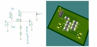
attenuator PCB
I like where you are going with this. A little attenuator brd could be an optional add to the Distinction. Would also allow us to tune the attenuation to our individual source. I too use the I2S->PCM. I am curious to see if this is why I can't get above 44.1 speed without overwhelming white noise. The guys running 384 on the tda were using the redbaron board after Ian brd which has John's attenuator circuit. I am not fussed by it as I am getting awesome sound at 44.1 which is 99% of my collection.
Heres something i think ill try this weekend if i have the parts. I think ill just try it on BCK first. Let me know if you spot any mistakes.
Cheers
I like where you are going with this. A little attenuator brd could be an optional add to the Distinction. Would also allow us to tune the attenuation to our individual source. I too use the I2S->PCM. I am curious to see if this is why I can't get above 44.1 speed without overwhelming white noise. The guys running 384 on the tda were using the redbaron board after Ian brd which has John's attenuator circuit. I am not fussed by it as I am getting awesome sound at 44.1 which is 99% of my collection.
Yeap, the regs are good but not sure the cells are fast enough ! Huge Z but alkaline cells and some Lipo ones ?
I really advise to go with the I2StoPCM : for me it's a no return point !
@ RyanJ :
I don't understand ; do you talk about bandwidth or transcient or impedance floor when you talk about not fast enough ?
Not clear to me ! What cap feeds the Darlington, transistors emitter follower of your shunt ? I mean Salas knows how to make a shunt regs, I would bet more to a non large enough bandwidth maybe on this particular shunt red to feeding a DAC ! Maybe worth to try the reflektor D ? And swap the one you use for the DAC for the analog stage ?
I don't know really as you have a very far better understanding of those things than I have !😱; e.g. I believed, greater distance on a I2S line could change the rise time !
PS : does the three or four inputs needs to have an equal input rise time or different rise time will create jitter... or there is no links between jitter and rise time between the emiiter and the receiver (dac chip) ?
As also attenuator must be close to the dac chip, could be better to try to putt smt resistor between the tda pins and the pcb leads ?
Last edited:
wire is inductive, yes... so the edges will be less steep.I believed, greater distance on a I2S line could change the rise time !
- Status
- Not open for further replies.
- Home
- Source & Line
- Digital Line Level
- Group buy/Interest list - TDA1541A Core board.