Yeap, the regs are good but not sure the cells are fast enough ! Huge Z but alkaline cells and some Lipo ones ?
I really advise to go with the I2StoPCM : for me it's a no return point !
The Z of the cell doesn't matter terribly, the regulator (with its caps) is what supply the load. The cell must have sufficient capacity to supply the input cap before the regulator. The current will flow in loops.
1. loop between the battery and regulator input cap
2. loop between reglator input cap and the regulator
3. loop between regulator output and the output cap(s)
4. loop between the regulator output caps and the capacitance at the load end
5. loop between capacitance and load end and the TDA1541(A) chip.
For fast loads the current will come from the closest capacitors and move further away as the energy being supplied increases (as caps are depleted).
So the Z of the battery only needs to have enough to charge the regulator input caps fast enough to not starve the downstream, which can be fixed by adding more capacitance at the regulator input cap.
The reason for taking this approach is the inconvenience of the complexity required by LiPO, LiFePO etc cells in their charging circuits and the difficulty to acquire the truly good cells of those types. Using more easily available battery and a regulator gives just as good (perhaps better) performance.
Chris
I like where you are going with this. A little attenuator brd could be an optional add to the Distinction. Would also allow us to tune the attenuation to our individual source. I too use the I2S->PCM. I am curious to see if this is why I can't get above 44.1 speed without overwhelming white noise. The guys running 384 on the tda were using the redbaron board after Ian brd which has John's attenuator circuit. I am not fussed by it as I am getting awesome sound at 44.1 which is 99% of my collection.
Hi Walter,
If my testing goes well ill start another interest list, finalise the design and get some PCBs made up depending on numbers. Hopefully ill have time to make a pcb this weekend, order the parts i need during next week and start testing the following weekend. I need more time in a day.
Yeap, the regs are good but not sure the cells are
@ RyanJ :
I don't understand ; do you talk about bandwidth or transcient or impedance floor when you talk about not fast enough ?
Its all related, in terms of power supply, the capacitors close to the tda pins will handle all the fast transients anyway
Not clear to me ! What cap feeds the Darlington, transistors emitter follower of your shunt ? I mean Salas knows how to make a shunt regs, I would bet more to a non large enough bandwidth maybe on this particular shunt red to feeding a DAC ! Maybe worth to try the reflektor D ? And swap the one you use for the DAC for the analog stage ?
I've heard about the reflektor D, have not read into it much but i would say it has a better transient response.
I don't know really as you have a very far better understanding of those things than I have !😱; e.g. I believed, greater distance on a I2S line could change the rise time !
I think you're right, but by how much im not sure. I know that I2S lines of the same length is important to make sure the delay is the same.
PS : does the three or four inputs needs to have an equal input rise time or different rise time will create jitter... or there is no links between jitter and rise time between the emiiter and the receiver (dac chip) ?
As also attenuator must be close to the dac chip, could be better to try to putt smt resistor between the tda pins and the pcb leads ?
Ill e-mail you a few e-books for you to read.🙂 They will answer your questions much better than myself.
Cheers! Friday drinks and bbq!

Last edited:
Perhaps, Ryan, a simple plug in board to fit some 'drilled out holes' on the existing board might be worth the initial trial for the input attenuator circuits - I think there some mention about feeding the returns to digital ground (rather than analogue gnd) and this may also require a separate +5V supply (or a simple RC or a CMx buffer)to the existing one .....
Is there such a thing as analogue & digital ground ? At the end of the day all will be connected together right. I believe that the route to good sound including logic circuit is to have a low noise stable power supply whose response is not over what is required for that circuit. This will ensure a minimal of thrash that's dumped to the ground. Ask any adc/dac designers whose worth his grain of salt & he will say Slow Down The Transmission. How is is done, well that's for all of us to experiment.
Cheers
Cheers
@ Hocho,
Thanks for those hints, I didn't know these modern regs coul manage the low impedance and the problem of transcient of the cells while staying with a low impedance at the output ! I really believed than the cells needed to have a lower noise floor !
Thanks Ryan,
I will read it.
About the transcient, I believe to know that the input cap which feed the darlington shunt is more important for the transcient than the output cap, mostly because the las is a local decoupling cap (doesn't work like a serie reg !) which only need to have a little capacitance and stay as fast than the cap at the input (which must ave both a huge capacitance and low esr as well, the low impedance is managed by the design or shunt chip like tl431 ?).
Some others flavor also with this last cap... (sorry for the french word).
Did you try before the output cap and the shunt a smt coil (47 to 100 uH ?) to damp the oscillation or a ferrite bead as it is not the analog signal ?
I'm not sure the REDBARON PCB is better, remember we do the Distinction to go for better than the redBaron as well !
I'm asking is the problem of Wlowes is not due to EMC or internal shielding, him dac is very complex... or just maybe because the BBB nano board!
In him shoes, but I surmise he did, I will remove this option by trying to feed the Wave I/O from a laptop and if the problem percist: a de casing ???🙁
Thanks for those hints, I didn't know these modern regs coul manage the low impedance and the problem of transcient of the cells while staying with a low impedance at the output ! I really believed than the cells needed to have a lower noise floor !
Ill e-mail you a few e-books for you to read.🙂 They will answer your questions much better than myself.
Cheers! Friday drinks and bbq!
Thanks Ryan,
I will read it.
About the transcient, I believe to know that the input cap which feed the darlington shunt is more important for the transcient than the output cap, mostly because the las is a local decoupling cap (doesn't work like a serie reg !) which only need to have a little capacitance and stay as fast than the cap at the input (which must ave both a huge capacitance and low esr as well, the low impedance is managed by the design or shunt chip like tl431 ?).
Some others flavor also with this last cap... (sorry for the french word).
Did you try before the output cap and the shunt a smt coil (47 to 100 uH ?) to damp the oscillation or a ferrite bead as it is not the analog signal ?
I'm not sure the REDBARON PCB is better, remember we do the Distinction to go for better than the redBaron as well !
I'm asking is the problem of Wlowes is not due to EMC or internal shielding, him dac is very complex... or just maybe because the BBB nano board!
In him shoes, but I surmise he did, I will remove this option by trying to feed the Wave I/O from a laptop and if the problem percist: a de casing ???🙁
Last edited:
Perhaps, Ryan, a simple plug in board to fit some 'drilled out holes' on the existing board might be worth the initial trial for the input attenuator circuits - I think there some mention about feeding the returns to digital ground (rather than analogue gnd) and this may also require a separate +5V supply (or a simple RC or a CMx buffer)to the existing one .....
Does all those local ground loop near the inputs pins and the analog gnd pin not a worst evil ?
I remember T. Loesch (or John) to say he made something with the 17 pF input capacitance and the shunts resistors to make a noise filter... but just don't remember where it is in the huge thread !
Jameshilij, you have a great experience with tda1541, how is yours today, what input and output stage ? Tubes iirc ?
regards
if V2
If a Distinction V2 : worth to putt some cut serie traces in the voltage leads like I asked during the V1 between plugs and power local decoupling caps to add ferrite beads, smt chockes or zero smt resistor if not used ? Near them, traces for modern ldo reg if no shunt used to have short ground loops ? (asked as well)
Have a brainstorming between each others members to improve the Ground pcb ? Four layers becomes very cheap those days ! One pcb like the distinction is less than 5 AUD by 100 parts ? Hiw much will cost a 4 layers ? I'm asking if ground on both side more than the analog ground star at the bottom is the best solution ? Better to use the top side only for continuous gnd plane (like the v1 with the merging of agnd and dgnd) and the bottom between pins for the analog gnd only (central island) in the middle of the tda pins or only for some local needs (return gnd path of digital lines ?)
And a delirious whisch pleasssssse: possible to add vias on the dem traces to allow old non smt decoupling caps with 2.5 mm pitch legs : would try a particular or two caps with leads/legs which could be as good if not better than ppps 🙂 : the legs could be soldered on the top side with vias only communacating with the bottom analog ground plane : caps will have the head in the bottom plane like the PPS caps are today !
Last edited:
+
- vias with a larger diameter for the caps leads with multiple pitchs for the voltage via to allow more caps choice and manage the inductances ?
- vias just behind the voltage plugs for an other entry decoupling cap (near the edge of the pcb but only if cutted traces for smt chockes/ferrite beads after)
- layout for a common smt chockes at each voltage rails ?
???? 🙂) I ask before all to be under control 😉 )
Ah Eldam, it's got a bit side-tracked at present - trying to complete some of the other overdue projects and the dac has been gathering dust on the shelf for awhile but keeping in touch with Ryan's developments - will get back to it soon
I have been using an Ayre Acoustic usb dac lately and have become accustomed to it's very neutral sound via the jRiver program, etc but there's just something about this old dac chip that keeps calling for attention - a trouble free, good performance usb input would be a welcome addition, instead of the card reader, IMO....
About the power supplies - I'm quite comfortable with the Salas shunts for this one but after reading a few of these recent comments, maybe it's a good time to explore some of the other options - I'm a bit doubtful of the basic 3 pin regulators as they've mostly not shown good results in the past, but stranger things have shown up with this particular chip and worth keeping an open mind
A series inductance? easy enough to try, I guess. I did try out some of John's C-Multiplier circuits awhile back and they seemed to work really well, but didn't persevere when the shunt regs appeared - similar thing with the 'dual lm317' arrangement.
Digital ground, eh? Well, looking at it from the point of view about current circulations and all that, this new attenuation scheme seems to be asking for a separate source of current to the dac chip's and this would mean that the return would also probably benefit from keeping the return away from the analogue supply, too - or at least, consider the possibility, when developing new boards, etc - could also be totally wrong about this too!
I recently received a rather surprising valve o/p stage design from 'our man from Milan' and this is getting some attention now by Ryan - I have been a bit disappointed in nearly all of the valve o/p stages for this dac, for one reason or another, but this one seems to offer great potential with a minimum of exotic parts.
All the best.
Eldam, do you refer tot the input capacitance of the TDA1541's digital inputs? According to the datasheet the are in the range of 12pF.. but also datasheets sometimes tell a different(=incorrect) story. 😕I remember T. Loesch (or John) to say he made something with the 17 pF input capacitance and the shunts resistors to make a noise filter... but just don't remember where it is in the huge thread !
yes. 17 pF iirNc 😱 ! You're surely right with 12 pF ! The main idea was to say to putt the resistive element near the pin to have the shortest possible ground loop, though some puts also resistor also at the output of the emitter (to avoid RF reflexion !) . But here this is not if it was a development from a to z : it's a coreboard, so some trade offs were choosen, And iirC this thime Ryan choosed simplicity to avoid some problems here as the resistive jitter path was discussed a lot at John's thread with a lot of revision (3 or 4 on this subject) !
T. seems to more agreed with the resistor approach! a zero ohms resistor if you don't want to use it et voilà ! Now, what value too choose if the value is dependant of the boards before as the I2StoPCM, or the Wave I/O, etc ? All have different output rise time ! But T. of course doesn't say all, he uses himself quad core resistor, caps, I surmise he could even take a tda1545a and makes it sounding good !
Well we can ask them all and encourage the published data asking them ! But also there are some more simple problems like boards interconnections which most of the time are too bad for I2S or too long !
That's why I'm for a democratic and holystic approach and a not closed one where everybody close the design in him corner ! Difficult thing but members are great here : Ian listen the inputs of the users, Distinction was the result of an open collaboration though the closing was maybe too rapid... but this is not like if it costed 7 000 bucks !🙂 Small money for the board quality, the most expensive was given fo free : the shared time of members : pure DIY approach and collaborative 🙂. We do have do it more ofently !
Last edited:
Hi Everyone,
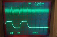
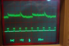
I've built a basic pcb for testing some i2s attenuation topologies. At the moment i've got 470r in series on all lines. Rise time looks pretty high, a bit over 35ns. (from ~2ns previously)
I took a few shots, there is something that stood out a bit - noise on the -15v supply has been lowered a lot.
Thanks for all the coments, im taking them all onboard. Answers to come, probably tomorrow. 😀
1541 psu bck noise 470ohm.JPG - With 470r
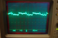
1541 PSU BCK noise.JPG - Before, without any series resistance.
I've built a basic pcb for testing some i2s attenuation topologies. At the moment i've got 470r in series on all lines. Rise time looks pretty high, a bit over 35ns. (from ~2ns previously)
I took a few shots, there is something that stood out a bit - noise on the -15v supply has been lowered a lot.
Thanks for all the coments, im taking them all onboard. Answers to come, probably tomorrow. 😀
1541 psu bck noise 470ohm.JPG - With 470r
1541 PSU BCK noise.JPG - Before, without any series resistance.
Attachments
Last edited:
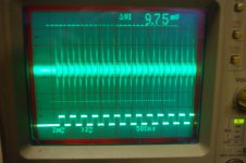
Heres a few more shots.
Output at my F5 playing 11025hz square wave -90db.
Looks a bit cleaner.
noise on F5 with 470r.JPG - with 470r
11025 F5 BCK.JPG - before, without a resistor
Output at my F5 playing 11025hz square wave -90db.
Looks a bit cleaner.
noise on F5 with 470r.JPG - with 470r
11025 F5 BCK.JPG - before, without a resistor
Attachments
Last edited:
Wow !
What is the board in front of the chip ? A wave I/O or I2StoPCM ?
What is the max rise time the TDA accept ?
What is the difference to your ears ? Softer in the highs ?
Did you try a 1 to 4 ohms resistor in serie between the output transitor of your -15v shunt reg and its last local output decoupling cap or if any before your -15v Nichicon decoupling cap (in serie on the plug) ? Does it give you a quiet - 15 V ?
🙂 super !
Last edited:
Ive got the i2s to pcm pcb. Not sure what the max rise time is, should say in the data sheet i guess.
Hard to comment on the sound because it does sound different now. And I was looking for a change, but - I'm getting more micro details. Lots of air. More experimenting needs to be done, and of course much more listening.🙂
Hard to comment on the sound because it does sound different now. And I was looking for a change, but - I'm getting more micro details. Lots of air. More experimenting needs to be done, and of course much more listening.🙂
Wow !
Did you try a 1 to 4 ohms resistor in serie between the output transitor of your -15v shunt reg and its last local output decoupling cap or if any before your -15v Nichicon decoupling cap (in serie on the plug) ? Does it give you a quiet - 15 V ?
🙂 super !
No, haven't played with any of that yet, took me about 12 hours to get to this point today... Making a pcb (Toner transfer method), populating, testing, and measuring. Good fun though! 😀
Nice job
Ryanj
Substantial impact.
I really enjoy seeing these experiments thru your pics. I would love to have a scope and do these experiments. Also appreciate how you jumped on this opportunity based on a curious inquiry. I look forward to implementing the results.
Walter
Ryanj
Substantial impact.
I really enjoy seeing these experiments thru your pics. I would love to have a scope and do these experiments. Also appreciate how you jumped on this opportunity based on a curious inquiry. I look forward to implementing the results.
Walter
Hi Walter,
Yeah i think visuals are a great way for us to judge what may be going on.
It seems obvious when you look at the pictures, that there is clearly a big impact. And the fact that I could sit down with a beer after and also hear a change just confirms this. More work to be done though, was just really curious what the outcome would be.
Ive got the i2s to pcm pcb. Not sure what the max rise time is, should say in the data sheet i guess.
Hard to comment on the sound because it does sound different now. And I was looking for a change, but - I'm getting more micro details. Lots of air. More experimenting needs to be done, and of course much more listening.🙂
Interresting !
If you listen to always the same material for yours experiments, the psycho effect is lowered maybe null ! I know it is boring always to listen to the same material during many years... but a fix point is needed !
More details... it's interresting and as we are not in the analog domain it's not at the price of a different tonal balance...good ! What resistor do you use ? your beautifull MILS you showed already... (the same as the 6k8) ?
Could be interresting to know the SDtrans rise time output to understand why John uses the values he gave !
CFT if you read us, did you know the rise time output of the SD trans reafder you use ? Could help maybe Tyan to choose an appropriate resistor value... I don't know if it can help ?
ah much more listening = much more beers.... an interresting concept as well 🙂
Last edited:
- Status
- Not open for further replies.
- Home
- Source & Line
- Digital Line Level
- Group buy/Interest list - TDA1541A Core board.