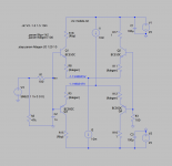
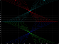
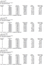
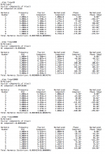
Here it is. A simple sim on a simplified dual ltp stage, with degen res varied, to see what their effect is.
I think the plot visual shows a lot.
I varied the degen res from 20 to 120ohms in 10ohms increments.
We can see the linear usable range widening a lot with increasing degen res values, however what we don't see there is the reduction of the gain that goes in the opposite direction.
Of course it's a compromise, and one important thing to keep in mind is that as Dr Leach pointed out, if we get out of the ltp's linear range, TIM can occur.
So by having sufficient degen value, we increase the linear range and we can make sure we don't get out of it, so as to prevent TIM.
There is however no point in going too far with high degen values, especially since the gain reduces as we increase those values.
The slew rate is also affected by this, so even more to keep in mind to compromise...
Attachments
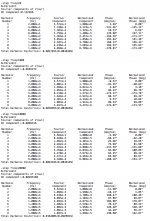
Switching from the 2N440x to the BC5x0 does bring a little more improvement, although not huge.
The vas bias is higher with the BC than with the 2N. (I kept the vas load res at 47, for better comparison)
The vas bias is higher with the BC than with the 2N. (I kept the vas load res at 47, for better comparison)
Attachments


Dropping from 2k2 to 1k very slightly improves things in both cases (2Ns and BCs), so 1k seems a tiny bit better.
I still haven't touched the vas load 47ohms res, so vas bias is still high.
I will now try reducing that vas bias, and since using 1k and the BCs are better, I'll use this as the starting point, and then I think if the dissipation drops enough in the vas, then perhaps we can also switch from the BD to the BC there as well, which should increase the gain in that beta enhanced vas.
This should be good and lower thd some more.
Attachments


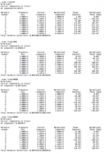
I didn't expect this much different in thd when lowering the vas bias.
I only dropped it to about 15mA (half the previous) using 100ohms on the vas load.
Will try 10mA now.
One thing looks useful here though, as the dissipation went down to a bit less than 115mW in the cascode (vas BD), and less than 80mW in the vas BD, so I think it could be done to use a BC instead of the BD there. Leaving the cascode BD as is.
This beta enhancement could help.
With the vas bias down to 10mA, that is obviously a good thing to do.
Attachments

Dropping the vas bias down to about 10mA continues to increase thd, significantly.
I wonder if this is a trade off that's worth it. Unless switching to the BC instead of the BD would increase gain enough to compensate.
The dissipation in the vas cascode drops to a bit less than 77mW and about 52mW in the other BD, which now quite easily could be swapped with a BC.
I think it's worth taking a look at this.
Attachments


Well, tough choice.
Going from BDs to BCs saves a tiny bit of pcb real estate, and the BCs are slightly cheaper than the BDs, but the thd is much higher this way and the swap from BDs to BCs in the vas doesn't compensate for all.
Doesn't seem worth doing so far.
The "richer" vas bias gave us much less thd.
Going from BDs to BCs saves a tiny bit of pcb real estate, and the BCs are slightly cheaper than the BDs, but the thd is much higher this way and the swap from BDs to BCs in the vas doesn't compensate for all.
Doesn't seem worth doing so far.
The "richer" vas bias gave us much less thd.
Attachments
Well, tough choice.
Going from BDs to BCs saves a tiny bit of pcb real estate, and the BCs are slightly cheaper than the BDs, but the thd is much higher this way and the swap from BDs to BCs in the vas doesn't compensate for all.
Doesn't seem worth doing so far.
The "richer" vas bias gave us much less thd.
I was not suggesting the BCs on the output VAS. I suggested 2n4401/3 because I it has higher current capability than the BC's, yet low Ccb. I suspect this won't matter much, but give it a shot. We get the most benefit by speeding up the first transistor using a BC.
I suspect that much of the increased distortion is due to reduced gain, caused by increasing the VAS emitter resistor. We need to keep a low value for high gain, perhaps. That's why I suggested a trim resistor to correct the bias, your R52/53.
Last edited:
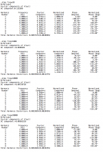
... A simple sim on a simplified dual ltp stage, with degen res varied, to see what their effect is. I think the plot visual shows a lot.
I varied the degen res from 20 to 120ohms in 10ohms increments.
We can see the linear usable range widening a lot with increasing degen res values, however what we don't see there is the reduction of the gain that goes in the opposite direction.
...one important thing to keep in mind is that as Dr Leach pointed out, if we get out of the ltp's linear range, TIM can occur.
So by having sufficient degen value, we increase the linear range and we can make sure we don't get out of it, so as to prevent TIM.
There is however no point in going too far with high degen values, especially since the gain reduces as we increase those values.
The slew rate is also affected by this, so even more to keep in mind to compromise...
Great post. This is very illuminating and the curves are great for conveying the findings.
I'm loving the lower distortion we got by reducing the LTP emitter resistors. One component change cut it in half. I'm rather in favor of keeping a low value and high gain, provided we avoid "TIM". The LTP and input filter must be considered together for this to happen.
Why mention this? I believe we should limit the input signal bandwidth in the passive input filter, to avoid instability. This is basic control systems theory and precedes the whole TIM debate by many years. I used a 3X larger than typical input filter for this reason.
I just took a look at the Leach amp, and noted he chose almost the same HF rolloff point (using 2k/390p rather than 1k/1000p), and I suspect his reasoning was similar. However, Leach chose much higher values of emitter resistors (300R), which at first glance I assumed was to avoid the need to match input transistors, but now I suspect he was avoiding TIM. It appears that he traded high gain and better distortion numbers away in return for higher transient handling capability -- which perfectly illustrates the tradeoff.
I would rather lower the HF rolloff in the input filter than tradeoff gain, bottom line. Should we look at this?
I was not suggesting the BCs on the output VAS. I suggested 2n4401/3 because I it has higher current capability than the BC's, yet low Ccb. I suspect this won't matter much, but give it a shot. We get the most benefit by speeding up the first transistor using a BC.
I was only exploring this because lowering the vas bias affords the option of using a higher gain low power device, and going from a TO126 to a smaller TO92 was kind of good for pcb layout as well.
And I was hoping the much higher gain of the BCs could do much better than with the BDs. Since lower vas bias was making this switch possible, I just thought it worth looking into.
I couldn't find any datasheets for the BDs giving any data on capacitance, for anything, no cob, no ccb, nothing, but I suspect the BCs, and likely the 2Ns to have lower cob and whatever, than the BDs.
I suspect that much of the increased distortion is due to reduced gain, caused by increasing the VAS emitter resistor. We need to keep a low value for high gain, perhaps. That's why I suggested a trim resistor to correct the bias, your R52/53.
Ok, that's going to be explored next.
Great post. This is very illuminating and the curves are great for conveying the findings.
Yes, I thought that plotted that way it really shows what's going on.
I'm loving the lower distortion we got by reducing the LTP emitter resistors. One component change cut it in half. I'm rather in favor of keeping a low value and high gain, provided we avoid "TIM". The LTP and input filter must be considered together for this to happen.
We're probably just fine with the input filter. One thing that contributes to keeping TIM low is making sure the input stage is fast enough to be able to handle the fastest transients the input filter can let in. The input filter limits the speed of the transients, so the input stage isn't taken by "surprise" by overly fast transients. Obviously we need to have enough slew rate to handle the fastest transient that can come in.
Why mention this? I believe we should limit the input signal bandwidth in the passive input filter, to avoid instability. This is basic control systems theory and precedes the whole TIM debate by many years. I used a 3X larger than typical input filter for this reason.
Agreed. And it goes beyond just stability, with the transient handling to prevent TIM from appearing. One other thing that comes into play for TIM is the output impedance, which should be as low as possible to maximize damping factor, so reactive effects from the speakers don't come back in through the output and the feedback to intermodulate. The lower the output impedance, the less effect there can be from what comes back from the speakers.
However, Leach chose much higher values of emitter resistors (300R), which at first glance I assumed was to avoid the need to match input transistors, but now I suspect he was avoiding TIM.
Yes. That was the whole point, and also he was applying the same principles as Matti Otala, which was to apply local feedbacks on each stage to make them more linear and have more moderate gain, and then have a weaker global feedback. So instead of using loads of open loop gain and strong feedback to minimize thd, he was reducing thd at each stage and counting less on global feedback to reduce thd.
I don't think the issue of transistor matching was his main reason for the higher degen res values. It was lower TIM.
It appears that he traded high gain and better distortion numbers away in return for higher transient handling capability -- which perfectly illustrates the tradeoff.
Yes. But there is a compromise to find, and I feel he may have gone a little bit too far in the direction of higher degen and lower gain.
For one thing, I have of course done some sims on his designs, and so far, it's not simulating quite as well as it's supposed to. The thd is higher than we achieve. So his own design can be tweaked a bit for better performance. Without sacrificing the efforts to lower TIM.
I would rather lower the HF rolloff in the input filter than tradeoff gain, bottom line. Should we look at this?
Well, we can look at everything in simulation, and learn a lot from it along the way.
What else would you like to explore?
We had some "incarnations" that already showed rather nice performance, at least for thd.
We may be able to find a compromise to reduce noise somewhat, but this is a difficult one to find, as each aspect is interdependent.
If we aim for more slew rate, we need more tail current, which causes more noise.
If we try reducing some resistor values that set gain, to reduce noise, other related values need adjusting as well, and the input impedance also gets affected.
We can probably tweak the input network a bit.
I have some simulations for discrete opamps which use very similar topo, with dual symmetric ltp, using the same BC5x0 devices, lower tail current, current sources and mirrors, some without the mirrors, and I have about 1/3rd the noise there.
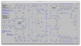
Let me recap my thinking on the VAS. Essentially, I took Self's reasoning to heart.
Self concluded that in the VAS, LF distortion arises mainly from Early Effect, while HF distortion from high Ccb. This guided my suggested changes to the VAS.
1. Lower Ccb: As a first step I suggested using lower Ccb transistors for the input of the Sziklai pair VAS. As expected, there was a slight benefit of lower HF distortion, all other things being equal. We did not address Early Effect yet.
2. Early Effect: The next step was the circuit I called Darlington VAS, which has a goal of eliminating Early effect on the input transistor, for reduced LF distortion. The input transistor of the Darlington pair has its collector fixed to ground to accomplish this. We are cascoding the second transistor for similar effect, though I suspect the first transistor dominates.
To minimize changes, I suggest keeping the BDs at first.
For whatever reason the circuit seems to like a bias of ~2.2v at the input transistor. I assumed about 1v drop on the emitter resistor plus 2 Vbe, or a total of roughly 2.2v.
Unfortunately increasing the VAS emitter resistor lowers open loop gain and raises distortion. You see this right away in your simulations. This will mask the beneficial effects of eliminating Early effect. If possible we need to keep the emitter resistor value low, hopefully 47R for comparison purposes (not the 100R I show, that was before your sim result). If we end up with 20ma of VAS current, so be it.
Anyway, that was my reasoning. The changes were directly aimed at particular causes of distortion. Hopefully if we keep the VAS emitter resistor low, the gain will be about the same and won't mask the effect of the two important changes.
Self concluded that in the VAS, LF distortion arises mainly from Early Effect, while HF distortion from high Ccb. This guided my suggested changes to the VAS.
I wish I had a deeper understanding of this. I can somewhat see what the ccb effet could be, but I have no sufficient understanding of what the early effect is.
I have read many things about this and so far I'm still not up to speed on this, but hopefully I'll learn something along the way here. This is great, and we are dissecting more and more details of how it works. All good!
2. Early Effect: The next step was the circuit I called Darlington VAS, which has a goal of eliminating Early effect on the input transistor, for reduced LF distortion. The input transistor of the Darlington pair has its collector fixed to ground to accomplish this. We are cascoding the second transistor for similar effect, though I suspect the first transistor dominates.
To minimize changes, I suggest keeping the BDs at first.
For whatever reason the circuit seems to like a bias of ~2.2v at the input transistor. I assumed about 1v drop on the emitter resistor plus 2 Vbe, or a total of roughly 2.2v.
Unfortunately increasing the VAS emitter resistor lowers open loop gain and raises distortion. You see this right away in your simulations. This will mask the beneficial effects of eliminating Early effect. If possible we need to keep the emitter resistor value low, hopefully 47R for comparison purposes (not the 100R I show, that was before your sim result).
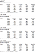
Alright, then here we are with that option you posted and using 47 instead of 100 on the vas.
If we end up with 20ma of VAS current, so be it.
Instead of adding a pot (100k), I just made that 33k variable and I ended up with 27k for about 12mA vas bias. A real circuit would not be using 2 more such pots, and it would never be possible to match their setting anyway, so I just used a normalized value. 27k worked, 22k was much too low, down in the 7mA range.
Anyway, that was my reasoning. The changes were directly aimed at particular causes of distortion. Hopefully if we keep the VAS emitter resistor low, the gain will be about the same and won't mask the effect of the two important changes.
Sounds quite reasonable.
With this much lower vas bias, we have similar thd result as earlier working versions. Not too bad, and now we'll see what that lower ccb device brings.
Attachments

With this second option, the vas bias goes to a bit over 13mA with the 33k resistors.
Having all the other values allows a good comparison, and although we have a little bit of thd improvement, more so in the middle, but not at the upper end, where it's a little worse.
Not what I was expecting.
Having all the other values allows a good comparison, and although we have a little bit of thd improvement, more so in the middle, but not at the upper end, where it's a little worse.
Not what I was expecting.
Attachments

I was curious to see the difference between the 2Ns and the BCs for the vas, so I just ran it.
Keeping the 33k for a vas bias that went up a little to closer to 15mA.
Take a look at the rail balance! wow! just 32uV out of balance!
Anyway, the BC does a tiny bit better than the 2N, and I rechecked on the dissipation, which is around 90mW, so perhaps they would run a little warm over time.
Good to compare. And the dissipation isn't much lower with the 2Ns.
Attachments
Trying to figure out what the datasheet mean when it comes to capacitance.
Some datasheet don't even mention anything about this. For example the datasheets that I have for the BD139/40 don't mention any capacitance, from any manufacturer.
And then some mention different values but not using the same terms or symbols to express them.
Example, fairchild's bc5(46-50) datasheet mentions an output capacitance, with symbol Cob, and input capacitance with Cib, and nothing really says what this actually pertains to. I assume the input capacitance should relate to the base-emitter junction, because this is basically the input. But I don't see the output capacitance as being for the base-collector junction, as this really isn't an output, and if this is for the collector-emitter junction, is this really pertinent?
Now I look at the general semi datasheet for the 2N4401, and there is no mention of input/output capacitance, and they use base/emitter and base/collector with Cebo and Ccbo respectively, which is more explicit and we can't mistake which junction this pertains to.
Why the different symbol? beats me! But some must be in common, as there aren't that many junctions in a bjt to begin with.
For one thing, if I'm right to assume that input capacitance is the one in the base-emitter junction, then the Cebo from some are the same as the Cib from others.
That leaves one Cob to figure out. Would that really be the base-collector junction? If so, then Cob is also Ccbo.
This lack of uniform convention can be so confusing.
If any of this is how I understand it as above, then the 2N4401 has 30pf (max) on b-e while the BC550 has 9pf (typical).
This would make the BC better, capacitance wise, than the 2N.
But there again there is a fuzz factor from one maker to the other, where one states only a max value, and the other only a typical one. More confusion and blurriness.
It seems that for the VAS, varying Cbc with Vce is a major HF distortion source. By the way, the acronyms vary, but I consider Cbc, Ccb, Cbco, and Cob to be nearly identical. I will use Cbc in blithe ignorance of the nuances. At any rate, this is a critical parameter for the VAS (while Cbe is not). It turns out that the BC parts have low Cbc, but many of the other ones we are interested in lack specs on this parameter.
In your last post you lament the sparse specifications of small signal transistors. You are correct. Very few parts have full specs. One of the reasons I like the 2N4401 is because it has a full spec, even though the part is ancient. It's an exception. Most data sheets are very sparse. We have to live with that.
I suspect that most design these days is done in analog IC houses which have very detailed models of the typical parts they use, and in fact when they need something special, they invent it on the spot. The models are no doubt valuable proprietary information that can give a competitive advantage, so they are seldom freely shared. We owe a debt to Bob Cordell and others who do share models, as they were a lot of work to build.
Self assembled a nice table of published Cbc for several devices in his Sixth Edition of Audio Amplifier Design, Ch 7, p170. It is available online via google books, for a quick look, but this book is essentially mandatory for so many reasons that I bought it, even though I have earlier editions. Here is the page:
https://books.google.com/books?id=i...or different types of VAS transistors&f=false
More data has been assembled by our colleagues here on DIYaudio:
http://www.diyaudio.com/forums/solid-state/168851-transistor-data-sorting-3.html
Getting back to the VAS, it looks like a low Vcb part like the BC550/560 pair is a good candidate for the input device of the Darlington VAS. We may be forced to use the BD139/140 types for the output and cascode devices due to current levels. I say this because I suspect we will have to increase the VAS bias voltage from the present 1.9v to give more headroom to the LTP and mirror, as it may be too low. Before we had 2.2v. We need headroom here to keep the mirror out of saturation and for other reasons. In addition, the input device probably has the most effect, my hunch. The BD devices may suffice, subject to your sim results. It turns out that without heatsinks they take the same PC board space as TO92 parts, and their cost premium is slight since they are very high volume parts. Using them means we do not have to provide current limiting on the VAS, which I would include otherwise.
We can get back some headroom in many ways, by simply decreasing the R in our front end power filter, by reducing LTP current, by adding a diode in the emitter leg, or by increasing the bias voltage using the trim pot. I'll simply do the first in the schematic below.
Another simplification I'm considering is to use the resistor ladder feeding the current sources as the reference level for the VAS cascode base. The voltage is about right, and provided we don't introduce problems that is probably a worthwhile simplification. I'll hold off until the next Rev, because I want to have only one variable at a time.
Attachments

I was curious to see the difference between the 2Ns and the BCs for the vas...
Keeping the 33k for a vas bias that went up a little to closer to 15mA.
Take a look at the rail balance! wow! just 32uV out of balance!
Anyway, the BC does a tiny bit better than the 2N, and I rechecked on the dissipation, which is around 90mW, so perhaps they would run a little warm over time.
Good to compare. And the dissipation isn't much lower with the 2Ns.
Interesting. I would not have thought to run this combo. Provided we don't exceed the 100ma current limits, this is very interesting. Unfortunately, we might at the extremes, in which case we need a current limiter on the VAS.
We owe a debt to Bob Cordell and others who do share models, as they were a lot of work to build.
I second that! 🙂
Cool! And I see he couldn't find the info for the BD139 either.Self assembled a nice table of published Cbc for several devices in his Sixth Edition of Audio Amplifier Design, Ch 7, p170.
I had seen this quite some time ago and forgot where it was.More data has been assembled by our colleagues here on DIYaudio:
http://www.diyaudio.com/forums/solid-state/168851-transistor-data-sorting-3.html
However, that list was meant to grow more, and so far, hasn't. It could be more complete. We all have data to share, which could be used to complete this.
If we are forced to keep the vas bias higher, sure. But with less than 15mA, it could be viable.We may be forced to use the BD139/140 types for the output and cascode devices due to current levels.
The BD139/140 are really beefier TO126 versions of the BC639/640, in TO92.
But as you mentioned, if we don't heatsink the TO126s, they don't really take up much more space on the pcb than the TO92. And they would operate cooler than their TO92 counterparts.
That's a plus, and anything extra that could eventually deteriorate the signal should be avoided if it can be.Using them means we do not have to provide current limiting on the VAS, which I would include otherwise.
This last incarnation has an issue with the bias.
Something is going on that causes a very abrupt drop of the bias, to very small amount, with a tiny variation of the bias adjustment.
Check those 2 screenshots, the difference of the cursor position at the bias spreader is tiny, and yet causes the bias to drop to nearly nothing.
So I couldn't adjust the bias to normal level.
I probably could adjust it, by going much further in decimals, but if this happens in a real build, the bias would be virtually impossible to adjust.
Attachments

We need to step back to a known working configuration. As near as I can see, the two recent changes were changing the power filter R from 100R to 33R, and changing the VAS emitter resistor from 100R to 47R.
I would suggest undoing the first, revert to power filter R of 100R. Verify operation.
If that is not working, revert to VAS emitter resistor of 100R.
I would suggest undoing the first, revert to power filter R of 100R. Verify operation.
If that is not working, revert to VAS emitter resistor of 100R.
- Status
- Not open for further replies.
- Home
- Amplifiers
- Solid State
- grounded collector amp