Are you guys simulating a good time?
Not really , bad models , cheap circuit , "value added trainwreck"( VAT) . Maybe keen can help. I'm playin' w/ the original now.It has a hard time beating a "baby 55" THD wise 🙁
That might just be funny, C2C.... I needed that 😎
Actually , the simulation can really stop. just build the "big stuff" that we know will work and "play" with the front end. Nico's right , I could of built 10 "flavors" of MPSA voltage boards by now , or a prototype/universal one.
OS
Last edited:
Wow, some really good points made.
See, I'm no leader! My only saving grace is when I go to sleep for 12 hours and Nico sneaks in to kick butt and drill the thread into shape.
OS, what are the fairchild part numbers for the MPSA models, or can you post them?
The CCS is NOT redundant. The voltage here is NOT constant, it varies exactly as the input voltage. It is FAIRLY constant, because the amp has so much gain and the input will be small in comparison. This is why the bootstrapped resistor CCS is quite possibly the BEST option. The transistor CCS is less reliable, and less stable, and more apt to generate stability problems. Don't mention the super/negative impedance CCS, it is horribly unstable in simulation.
BTW Nico, I did think about the single resistor current source. As I said above, the voltage across this resistor will vary with the input voltage. The modulation of LTP stage current will give rise to an AMPLIFIED MODULATION of the VAS. This modulation of VAS stage current will modulate Ft poles, open-loop gain, stability phase margin, output stage bias current, and will cause asymmetrical slewing.
I know some things well, but I don't know anything else. That why I am NOT the person to lead this thread.
Let's get the peripherals worked out now. How about we work on a high-power version first so we can easily downgrade it for lower power versions?
- keantoken
Here they are..
KST /KSP (below) Not getting good results with these. Can't get your lateral models to stop conducting at a normal Vgs threshold, either. maybe I'll use some fairchild models (laterals). have fun...
keen , I will reiterate the fact that the ppm designers (diy-audio engineering) use 2sc2240/a970/ ksc3503/a1381 exclusively. I remember being criticized for using MJE/MPSA ,etc. They must not think highly of the latter.
OS
Attachments
Last edited:
They aren't my first choice either, but I want to let others decide. Check out these models:
- keantoken
.model MPSW42 NPN(Is=34.9f Xti=3 Eg=1.11 Vaf=100 Bf=3.069K Ne=1.205 Ise=34.9f Ikf=.1435 Xtb=1.5 Br=6.726 Nc=2 Isc=0 Ikr=0 Rc=7 Cjc=14.62p Mjc=.4962 Vjc=.75 Fc=.5 Cje=57.62p Mje=.3536 Vje=.75 Tr=1.42n Tf=2.056n Itf=.9 Vtf=22 Xtf=270 Rb=10)
.model MPSW43 NPN(Is=34.9f Xti=3 Eg=1.11 Vaf=100 Bf=3.069K Ne=1.205 Ise=34.9f Ikf=.1435 Xtb=1.5 Br=6.726 Nc=2 Isc=0 Ikr=0 Rc=7 Cjc=14.62p Mjc=.4962 Vjc=.75 Fc=.5 Cje=57.62p Mje=.3536 Vje=.75 Tr=1.42n Tf=2.056n Itf=.9 Vtf=22 Xtf=270 Rb=10)
.model MPSW92 PNP(Is=40.74f Xti=3 Eg=1.11 Vaf=100 Bf=105 Ne=1.326 Ise=40.74f Ikf=.6228 Xtb=1.5 Br=4.15 Nc=2 Isc=0 Ikr=0 Rc=10 Cjc=31.63p Mjc=.5163 Vjc=.75 Fc=.5 Cje=88.56p Mje=.2744 Vje=.75 Tr=2.212n Tf=1.654n Itf=2.2 Vtf=22 Xtf=350 Rb=10)
.model MPSW93 PNP(Is=40.74f Xti=3 Eg=1.11 Vaf=100 Bf=105 Ne=1.326 Ise=40.74f Ikf=.6228 Xtb=1.5 Br=4.15 Nc=2 Isc=0 Ikr=0 Rc=10 Cjc=31.63p Mjc=.5163 Vjc=.75 Fc=.5 Cje=88.56p Mje=.2744 Vje=.75 Tr=2.212n Tf=1.654n Itf=2.2 Vtf=22 Xtf=350 Rb=10)
- keantoken
They worked good. This is what scares me about models for "old transistors". I now have acceptable performance without the cascode at the "backend" of the
VAS.(similar to yours)
OS
VAS.(similar to yours)
OS
OS, I would like you to check removing the miller cap on left side of the VAS LTP. In my simulation, losing this cap improved stability. My simulation also indicates removing the miller cap on the mirror hardly affects performance.
What is our goal? 100W? 200W? Let's make it something high, so that lowering the power if necessary will be trivial.
- keantoken
What is our goal? 100W? 200W? Let's make it something high, so that lowering the power if necessary will be trivial.
- keantoken
Got it... (below , attachment 1)
200W + is a good power goal
New models , too...
Even have the exicon laterals... 🙂
we might use this for our Jfet , PMBFJ620,115 NXP Semiconductors JFET

25v Vds high gain , trying to find a model for it.
VERY stable , very linear (full wilson w/mpsa42's)
2.8mA LTP ,6ma VAS , 100mA lateral bias.
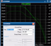
.05% thd 20- .01% 1k /40v p-p (Bode is below).
60 volts for OPS and 80 volts for LTP/VAS like Nico recommended.
all is better now. 🙂 Focused 😱😱 Have stayed true to the original.
OS
200W + is a good power goal
New models , too...
Place these in your LT mosfet library..MODEL 2SK1058 NMOS (VTO=403.969M KP=20U L=2U W=29.7482M GAMMA=0 PHI=600M
+ LAMBDA=184.988F RD=60.8251M CBD=2.56138N IS=10F CGSO=1.13517N CGDO=1.13517N
+ TOX=0 NSUB=0 TPG=1 UO=600 RG=50 RDS=1MEG )
.MODEL 2SJ162 PMOS (VTO=842.193M KP=20U L=2U W=21.3317M GAMMA=0 PHI=600M
+ LAMBDA=20.7067M RD=837.199M CBD=2.96862N IS=10F CGSO=1.13517N CGDO=1.13517N
+ TOX=0 NSUB=0 TPG=1 UO=600 RG=50 RDS=1MEG )
.MODEL ECX10N16 NMOS (LEVEL=1 VTO=-66.415M KP=20U L=2U W=76.3794M GAMMA=0
+ PHI=600M LAMBDA=3.44617M RD=244.181M RS=178.517M IS=10F CGSO=100P CGDO=100P
+ TOX=0 NSUB=0 TPG=1 UO=600 KAPPA=200M RG=367.902 RDS=16.0012K )
.MODEL ECX10P16 PMOS (LEVEL=1 VTO=56.1959M KP=20U L=2U W=49.9039M GAMMA=0
+ PHI=600M LAMBDA=16.6941M RD=458.28M RS=214.674M CBD=1.00674N IS=10F CGSO=100P
+ CGDO=100P TOX=0 NSUB=0 TPG=1 UO=600 KAPPA=200M RG=35.8793 RDS=1MEG )
Even have the exicon laterals... 🙂
we might use this for our Jfet , PMBFJ620,115 NXP Semiconductors JFET
25v Vds high gain , trying to find a model for it.
VERY stable , very linear (full wilson w/mpsa42's)
2.8mA LTP ,6ma VAS , 100mA lateral bias.
.05% thd 20- .01% 1k /40v p-p (Bode is below).
60 volts for OPS and 80 volts for LTP/VAS like Nico recommended.
all is better now. 🙂 Focused 😱😱 Have stayed true to the original.
OS
Attachments
Hey OS, Hfe linearity doesn't matter much for the spectrum in simulation, as I have found, until you get really low distortion. I think Hfe-Vce characteristics are more important, and SPICE models this rather generically (at least the models do - I will check this out).
- keantoken
- keantoken
Attachments

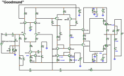
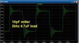
OS, youi have already modified the amp without telling us why. (I am asuming the get better phase margin). Dump the 8 ohm load and replace it with say 5uF and run another plot to check if it is shunted into oscilation. Post it so we can see.
OS I have learned something really cool with simulation. You simulate two schematics, the original (which you do not change at all) and the one you are working with and you can switch between them. Problem is when you are in supper hyped up mode you haphazardly change without keeping track.
OS I have learned something really cool with simulation. You simulate two schematics, the original (which you do not change at all) and the one you are working with and you can switch between them. Problem is when you are in supper hyped up mode you haphazardly change without keeping track.
200 watt is good. But just check voltages confirming that capacitor ratings do not jump to 100V being expensive for the community. Maybe 150watt, keeps all large capacitors at 63V and affordable.
Hi Kean, sorry I do not follow what you mean by linear Hfe. Ic/Ib is not linear, else we will have perfect zero distortion amps.
OS, for Nico's test remove the zobel. One of our goals is to not need a zobel.
Also, I don't think C9 is necessary. In all my simulations it decreases performance.
- keantoken
Also, I don't think C9 is necessary. In all my simulations it decreases performance.
- keantoken
This "http://www.linearsystems.com/datasheets/LSK389.pdf" could be used too.
Dual monolithic low noise N JFET.
dado
Dual monolithic low noise N JFET.
dado
Nico, in my experience the exponential Vbe is more responsible for distortion - just look, every transistor has to have some sort of resistance across it's Vbe to bias the preceding stages, and if not we're basing the entire circuit's linearity on one or two junctions in the differential/LTP. In my experience the nonlinearity coming from the nonlinear bias with output across this resistor is more than that of the Ib, as long as the transistor is operating in its linear range.
I was not talking about the Hfe-Ic curve, I was talking about the Hfe-Vce curve. This curve is one of the things which makes transistors unique, and it is also not modeled, and it's impact on harmonics not seen in simulation.
- keantoken
I was not talking about the Hfe-Ic curve, I was talking about the Hfe-Vce curve. This curve is one of the things which makes transistors unique, and it is also not modeled, and it's impact on harmonics not seen in simulation.
- keantoken
Last edited:
Hi OS, are you guys hell bent on using the input FETs, what are the advantages? Have you tried replacing the FETs with 2SA970 transistors and instead of the cascode use mirror.
The symmetrical VAS is not as effective with a current mirror - we might as well remove half of the VAS and replace it with a CCS, and then it would be a Blameless.
- keantoken
- keantoken
Kean, Rico somebody
Please post the final schematic for the Front END power supplies (+/-) that will be used
Thanks
Please post the final schematic for the Front END power supplies (+/-) that will be used
Thanks
"super hyped- up mode" 😀
I'm on a"chill pill" now. More objective. 🙂
Below is 4.7uF load w/ 2khz SW. Damped ringing , not outright oscillation.
The reason for the wilson is that with the resistor instead of the cascode on the VAS a single simple mirror provided insufficient gain even with less degeneration... The wilson does. We are using to-92's ,2 more wont hurt for X10 better perfomance.
Fet's are "audiophile cheddar" everybody loves them despite higher THD. I personally don't mind BJT differentials , they can be made to perfection.
Don't like current mirror's ... Keen ?? The VAS would lose a lot of gain without them. Then you would need to add one to the Differential. I am just trying to keep the "goodman" original flavor.
Keen ... better JFET models 2sk170/389
OS.MODEL LSK389A NJF
+ BETA = 0.0378643 VTO = -0.4025156 LAMBDA = 4.783719E-3
+ IS = 3.55773E-14 N = 1
+ RD = 10.6565 RS = 6.8790487
+ CGD = 3.99E-11 CGS = 4.06518E-11
+ PB = 0.981382 MJ = 0.794653 FC = 0.5
+ KF = 0 AF = 1
*
.MODEL LSK389B NJF
+ BETA = 0.0350699 VTO = -0.5375582 LAMBDA = 4.951E-3
+ IS = 2.76212E-14 N = 1
+ RD = 7.82168 RS = 6.9525888
+ CGD = 4.36E-11 CGS = 4.36E-11
+ PB = 1.2 MJ = 0.8892205 FC = 0.5
+ KF = 0 AF = 1
*
.MODEL LSK389C NJF
+ BETA = 0.0278541 VTO = -0.800434 LAMBDA = 0.0122435
+ IS = 2.45217E-14 N = 1
+ RD = 12 RS = 5.8 CGD = 4.22E-11
+ CGS = 4.23E-11 PB = 0.9265487 MJ = 0.6098477
+ FC = 0.5 KF = 0 AF = 1
.MODEL LSK170A NJF
+ BETA = 0.0378643 VTO = -0.4025156 LAMBDA = 4.783719E-3
+ IS = 3.55773E-14 N = 1
+ ACM = 0 RD = 10.6565 RS = 6.8790487
+ CGD = 3.99E-11 CGS = 4.06518E-11
+ PB = 0.981382 MJ = 0.794653 FC = 0.5
+ KF = 0 AF = 1
*
.MODEL LSK170B NJF
+ BETA = 0.0350699 VTO = -0.5375582 LAMBDA = 4.951E-3
+ IS = 2.76212E-14 N = 1
+ ACM = 0 RD = 7.82168 RS = 6.9525888
+ CGD = 4.36E-11 CGS = 4.36E-11
+ PB = 1.2 MJ = 0.8892205 FC = 0.5
+ KF = 0 AF = 1
Attachments
Last edited:
Good idea lets see what we have got. Problem is going off in a tangent is to easy. OS post what you have, both original and our design. Lets discuss the merits and disadvantages then settle on an outcome.
Kean, don't throw stones in the bush further that we are at present you will have an opportunity when we get there.
Lets stick to slow progress, some sleep while others are awake, the earth is not flat so the sun does not shine everywhere at the same time. If we want the best amplifier in the world it will not be done by next week-end.
OS this is already pretty pleasing, that means there is no instability per say, ringing is underdamping, this can be fixed, but not now.
Worse case is about 2uF in series with one ohm. We are okay. Lets move on. OS publish the current schematic so all are on the same page.
Kean now it is time for your comments regarding the VAS.
Worse case is about 2uF in series with one ohm. We are okay. Lets move on. OS publish the current schematic so all are on the same page.
Kean now it is time for your comments regarding the VAS.
- Home
- Amplifiers
- Solid State
- Goldmund Mods, Improvements, Stability