OS I take it there is no zobel and there is no compensation anywhere, or is it as per original Goldmund.
nearly finalized .. comments/suggestions??
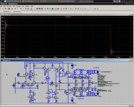
A nice little amp. .01% 1k .02@10k .04@20k - 85V/us symmetrical slew w/ 15pF millers. All this while remaining stable into a strait 4.7uF load or a 2R/2uf @ that same 90V square wave. Bandwidth would be about 500kHz without input filtering.
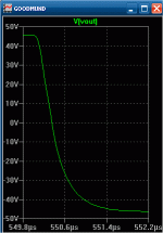
See the rise/fall Slew (plots 1and 2) AND the standardized schema -
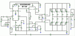
(attachment3). R's and C's up to 20 are the voltage stage... R's and C's descending from R99/C99 are the power stage.
R80/79 is the biasing setup. R79 will only allow about 250ma per device in case R80's wiper (1K- 25 turn Vbias) fails.
OS
A nice little amp. .01% 1k .02@10k .04@20k - 85V/us symmetrical slew w/ 15pF millers. All this while remaining stable into a strait 4.7uF load or a 2R/2uf @ that same 90V square wave. Bandwidth would be about 500kHz without input filtering.
See the rise/fall Slew (plots 1and 2) AND the standardized schema -
(attachment3). R's and C's up to 20 are the voltage stage... R's and C's descending from R99/C99 are the power stage.
R80/79 is the biasing setup. R79 will only allow about 250ma per device in case R80's wiper (1K- 25 turn Vbias) fails.
OS
Attachments

Looking good OS!
One question regarding offset adjustment, instead of the present arrangement how about making R9 adjustable......pro's and cons?
We should be able to go to board pretty soon. Thgis should be vastly superior to the Goldmend if implemented correctly. Nice work.
Regards,
Jam
One question regarding offset adjustment, instead of the present arrangement how about making R9 adjustable......pro's and cons?
We should be able to go to board pretty soon. Thgis should be vastly superior to the Goldmend if implemented correctly. Nice work.
Regards,
Jam
Last edited:
We should be able to go to board pretty soon.
would be nice with a long narrow output board, with drivers
and a matching frontend board, mounted vertical right above, flat on heatsink
with connections carefully and logically positioned, to give ultra short wire
each board design will be much better
and final inner box layout very compact, with more distance to trafos, and less noise problems

Power out @ 8 ohms?
Power out should be a conservative 200W+ 8R.. each 2SK/J will have about 2A SOA / 1sec @ 60V rails. This is about 1.5 times my BJT ops's. The limiting factor will be the lower rail voltage. The OPS will most likely do up to 275W with 70V rails and still be within it's SOA at 8R.
By Tinitus - would be nice with a long narrow output board, with drivers and a matching frontend board, mounted vertical right above, flat on heatsink
with connections carefully and logically positioned, to give ultra short wire
EXACTLY as I envisioned , the output board can be VERY narrow with no Vbe. All it will have is the 2 drivers/8 laterals / caps and trimmer/resistors. The Voltage stage will be best like my mongrels (100mm X 75mm) with the standard euroconnector /PCB pin attachment method. this will be cool for me as I can power the laterals with any of my amps.
I was thinking Nico's regulator as a separate board or on the OPS board itself.
OS
Can you probide a final freq/phase plot and also a THD plot at 1, 10 and 20 kHz into 4 and 8 ohm loads. Finally print the power dissipation of the devices, I am particularly interested in Q10 and Q7.
What is the purpose of L1 // R98 = .22 Ohm? should R98 not be a much higher value?
What is the purpose of L1 // R98 = .22 Ohm? should R98 not be a much higher value?
Goodmund by OS? I guess when Kean changes a resistor value it will be called Greatmund by Keantoken, and another, and yet another.....
First, since we are simulating, we need to have comparable simulations. OS, could you post the files?
OS, I keep saying C6 is not necessary, and you keep putting it in without addressing this, at least publicly. Test phase margin with and without C6 - which allows for lower miller capacitance at the same stability?
Also, C2 being 220p decreases BW at the start. To see the circuit's actual behavior, you should replace this with something much smaller, say 15p MAX, only enough to swamp out the Jfet's capacitance.
What are we looking for when we look at ringing plots? Let's inspect the mechanics.
1: ringing occurs because the amplifier has a parasitic output inductance, formed by the slowness of the feedback loop and/or devices used. When combined with a capacitive load, it resonates.
2: This ringing is damped by any series resistance. Most often the amplifier's. Amplifiers with less series resistance (those with high OLG) will ring longer.
3: If the parasitic inductor is made very large, ringing is eliminated. However this makes the amp very slow. Alternately, if we make the inductor extremely small, ringing is also eliminated because inductance becomes small in relation to output resistance.
From this I believe we can see that to eliminate ringing entirely through use of compensation does not necessarily mean a better performing product. Lowering open-loop gain will increase output impedance and dampen ringing some, at the cost of LF distortion. Increasing speed will decrease ringing as long as the amp still has adequate phase margin, but if it was practical we would have done it already.
If our aim is to have the circuit reasonably stable without a Zobel, then we should shoot for higher output impedance and lower output inductance. This means lower OLG, which can easily be done by using/increasing degeneration, and also means finding a faster way to compensate the amp, if possible.
Actually Nico, I had settled on the name "New Gold".
- keantoken
Not sure why I wrote the above, I think stable into 5uF is enough.
You have me right OS, no current mirror. Gain will increase? Yes, of course. LF performance will increase? Yes. Not so sure about HF performance, since this depends on the compensation values.
If we use a mirror, there will suddenly be a huge gob of gain focused exclusively at a high-impedance junction of two collectors, to the base of one of the VAS transistors. ALL of this extra gain will depend solely on the quality of the transistors and wiring. This gain at LF will depend solely on the Beta of the VAS, and at HF will depend on the Cob of the transistors used. I do not like to gamble with specs like this.
I agree with the schematic so far, except for C6, and I believe in a beta-enhanced VAS.
Other than this, I get the feeling a LOT of people are going to want to change degeneration, Jfets used, CCS current, cascode voltage, etc. So we MUST make the board suitable for many Jfets, degeneration, CCS current and we should write up a guide for how to do so without breaking it.
- keantoken
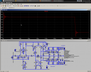
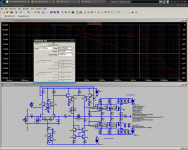
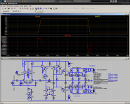
Here is my schematic with the VAS buffer.
As you can see the ringing is much faster; this is because the amp is faster, indicating smaller output inductance. The capacitance seen by the VAS is buffered from the frontend through the 2N5769's, making it much faster. Unity gain is now 2.6MHz!
I think I'm not going too fast...?
- keantoken
As you can see the ringing is much faster; this is because the amp is faster, indicating smaller output inductance. The capacitance seen by the VAS is buffered from the frontend through the 2N5769's, making it much faster. Unity gain is now 2.6MHz!
I think I'm not going too fast...?
- keantoken
Attachments
Oh, I'm sorry. I meant current mirror in the input stage, not the VAS. My apologies. Current mirror in the VAS is fine.
- keantoken
- keantoken
Okay, many arguments have been made in lieu of drivers.
The drivers have been biased at about 15mA. I bias them higher than the VAS, so they're not redundant. They require base stoppers, but this hardly impact performance.
What is left is an amp with smooth, textbook curves. I will post distortion figures later.
Here is it with drivers. Guys, this amp is very stable, working really well right now. I think this schematic could be PCB'd right now, what do others think?
- keantoken
Attachments
Here are the figures. For THD:
Phase shift into 4 ohms at 100KHz is 2.4 degrees.
- keantoken
1KHz:
60V into 4ohm: .000484%
60V into 8ohm: .000454%
10KHz:
60V into 4ohm: .003345%
60V into 8ohm: .002995%
20KHz:
60V into 4ohm: .006648%
60V into 8ohm: .005958%
Phase shift into 4 ohms at 100KHz is 2.4 degrees.
- keantoken
- Home
- Amplifiers
- Solid State
- Goldmund Mods, Improvements, Stability