
peppennino, the 10uF motor run caps are used as coupling caps. The input cap is bypassed with a Russian cap and the output cap bypasses the 10mF electrolytic coupling cap.
Sorry, I made mistake in reading... Perhaps I intended SSJ

F2J is a truly keeper! Great!

You can see all the advantages of the power jfet compared with the Irfp240 explained by mr. Pass in the F2J document. “Much lower distortion” ")
FIRST WATT
Hubert
FIRST WATT
Hubert
Last edited:

It’s alive!! I can definitely see why this is a perennial favorite to First Watt fans! Thank you once again Cody and Nelson!!
Hi Randy,
Do you know what values you ended up using for r33 and rdg?
Hubert
I built for Single Ended Input.
Post 1394
https://www.diyaudio.com/forums/pass-labs/151909-firstwatt-j2-140.html#post5906779
IF you use the amplifier with single ended input, i.e. -Vin = 0V, then R3 should be 10k, R4 should be 100k.
IF however you are using symmetrical inputs, i.e. -Vin = -(+Vin), then those value as published will load the source symmetrically.
Here's what I did:
ID Description
R1 10k
R2 100k
R3 10k
R4 100k
R5 10k
R6 100R SMD 0204 melf type - Bought extras for SMD solder practice
R11 & 12 0R82 3W
R13 & 14 1R1 3W
R15 & 16 0R22 3W
R33 300R
Rg4 10R
Rg5 10R
Rdg (pot) 50R Ended up buying 500R. Can't remember why??? Intially set at 250R and dialed it in at startup procedure. It took many turns.
C2 10uF
C4 5pF
Q1 2SK170BL bought from Punkydawgs
Q2 2JS74BL bought from Punkydawgs
Q3 2JS74BL bought from Punkydawgs
Q4 IRFP240
Q5 SJEP120R100 Thanks Nelson Pass!
IC1 CNY17-3 (SMD) Bought extras for SMD solder practice)
Setup procedure was from looking at the J2 thread. My notes
Leave power devices out. Power up PCB.
For Rdg, adjust the voltage across 300 ohm R33 to 1.275V vdc with inputs IN+ and IN- to ground.
Then with the power devices installed, Rdg adjust for DC offset across speaker terminals. as a fine adjust after thermal stability.
8.5mA refers to the current in Q1, and NOT R33.
R33 will normally see half of that, i.e. 4.3mA.
Therefore go for 1.275v on R33 @ 300R
Hindsight / Lesson learned, perhaps don’t solder the jumper wire on the PCB, and use those 2 points as test points to use DMM in Current / Ammeter mode.
Don’t install output semis, adjust pot to get 8.5mA. When at 8.5mA, install jumper, install semis. Fire up, measure offset, adjust, warm up, re-adjust offset at temp.
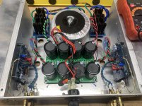
I spent a little time checking out the J2 today.
Voltage across R15&16 = 150mV
Voltage across R11&12 = .56V
Voltage across R13&14 = .73V
Looks like 1.36A per channel.
Gain looked around 19dB ish
Offset <10mV
2nd order distortion 2.83V into 8R = 0.036%
3rd order distortion 2.83V into 8R = 0.017%
I'm going to call this one done and enjoy the music!
Voltage across R15&16 = 150mV
Voltage across R11&12 = .56V
Voltage across R13&14 = .73V
Looks like 1.36A per channel.
Gain looked around 19dB ish
Offset <10mV
2nd order distortion 2.83V into 8R = 0.036%
3rd order distortion 2.83V into 8R = 0.017%
I'm going to call this one done and enjoy the music!
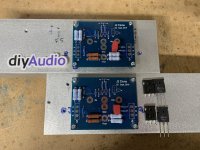
I’m finally getting to my J2 project. It’s going into a chassis that had a F5 clone in it. So the power supply is good to go.
Thank you once again Cody & Nelson!!!
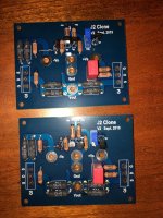
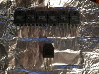
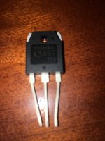
I bought the J2 clone PCB's from you, finally have them completed. It has been quite the adventure finding genuine Toshiba 2SK3497 MOSFET's. I bought two from a seller in the UK, one was tested as a MOSFET and the other was dead on arrival. Of course seller stated "they were tested good when I shipped them", oh well.
I found a very reliable source for the real thing, Tomo Watanabe-san in Tokyo, since I bought 4 TOKIN THF-51s from him I sent him an email seeing if he had any. He wasn't to thrilled selling and shipping just two for me, so I bought 6, glad I did, they don't look like the other ones I bought. My component tester also gave different results than the six from watanabe-san.
I included a pic of the UK sourced MOSFET, does it look real?
Thank you, Nelson, Cody, Randy and EUVL, no way could I have gotten this far.
Attachments
- Home
- Amplifiers
- Pass Labs
- Giveaway - SJEP120R100 pair