OK, I have another question.
D1/D2 are not in the BOM, but they are present in the input stage schematics and on the PCB. What should I do about them?
D1/D2 are not in the BOM, but they are present in the input stage schematics and on the PCB. What should I do about them?
Hi
refer to section 9 of the FSSA build manual for zener diodes D1/D2:
”….Assuming that most of the jfet IDSS within range of a BL grade or B grade will be <12ma max then I target to have no more than 150mW dissipation max (with no heatsink) for J1-J2-Q1-Q2. PSU voltage divided by 2 (using zener voltage of about half of PSU voltage) gives about equal heat dissipation between J1/J2 and Q1/Q2. Note if your IDSS > 9ma then you can add a small heatsink on top of J1/J2/Q1/Q2 to limit transistors temperature. Since the LSJ74 has a max voltage of 25Vdc the Zener max voltage is 24Vdc with 0.65V additional margin because of Q1/Q2 Vbe voltage drop.
Therefore the PSU max voltage supply can be determined as such: 175mW/ 7ma= 25Vdc, then x 2 gives 50Vdc, +/- 50Vdc as PSU. It is also possible to increase the PSU voltage to +/-55Vdc provided the IDSS of J1/J2 is <= 9ma and small heatsinks are used on top of J1/J2 with D7/D8 zener voltage at 24Vdc…”
Fab
Sorry, it's still not clear for me. Should I use D1/D2 with half voltage value of PSU? And the same is true for D7/D8?
The schematics in the Input Stage Test section show D7/D8 as 22v and D1/D2 as 12v.
The schematics in the Input Stage Test section show D7/D8 as 22v and D1/D2 as 12v.
Ok you confused me when you said D1/D2 in the input stage but they are rather the ones at the gate of the mosfet output stage… as per schematics they are required for mosfet protection (in case of overload) and they are 12VDC And no relation at all with PSU voltage. You are the first one noting it was missing from the BOM….thanks for that. You can use an alternate Zener voltage value from 9.1VDC to 13VDC max for D1 and D2 without effect on the sound in normal operation.
As for D7/D8 in the input stage, as per manual they must be half the PSU voltage with a max of 24VDC as per the “p. “ note of BOM list. There is even an example in the note. What is your PSU voltage?
Fab
As for D7/D8 in the input stage, as per manual they must be half the PSU voltage with a max of 24VDC as per the “p. “ note of BOM list. There is even an example in the note. What is your PSU voltage?
Fab
Last edited:
Now it makes sense, thanks!
My PSU is still in the works but I expect its voltage to be about 49-50VDC.
By the way, there is another inaccuracy in the BOM: # 28 for R35, R23, R24, R11, R12 requires 10 pcs for 2 channels, not 6. And # 18 for R33, R34 requires only 4 pcs, not 6.
My PSU is still in the works but I expect its voltage to be about 49-50VDC.
By the way, there is another inaccuracy in the BOM: # 28 for R35, R23, R24, R11, R12 requires 10 pcs for 2 channels, not 6. And # 18 for R33, R34 requires only 4 pcs, not 6.
Last edited:
Ok then you can use 24VDC zener for D7/ D8.
I will update the BOM for quantity of pieces as per your indications, thanks.
Fab
I will update the BOM for quantity of pieces as per your indications, thanks.
Fab
Gentlemen,
I am into AB(ish) amplifiers these days and your project is definitely a very appetizing alternative to my already completed / under construction / under consideration HB / Wolverine, PassAB and Q17 builds. May I ask you to prompt me to the latest documentation (schematics, specs, non-obsolate BOM, PCB layout)?
Thank you in advance,
Miklos
Hi Miklos
thanks for your interest.
Both FSSA-1 (mosfet drivers) and FSSA-2 ( bjt darlington drivers) have obsolete drivers. Note that the FSSA-2 drivers could be replaced with TIP-112/117 without other parts changed. However, the sound result difference (with these drivers) has not been assessed yet by anybody….. overall it should be minimal compared to overall design based on differences obtained between FSSA-1 and 2. Schematics is provided at post 9 of this thread using obsolete drivers. I can provide some tweaks to be done depending on the sound tonal balance you prefer. Documentation can be provided by message but for PCB layout I sell the PCB at reasonable price.
Fab
Dear Fab,
thank you for your detailed answer. I am definitely interested in this project and would appreciate your quotation for the PCB (2 channels) & documentation in PM. At this point I have just two more general questions: assuming the 400-600mA bias discussed in the thread, how much cooling is required? Can I get along with a 2U chassis or is a 3U necessary here? The schematics indicates 48V rails. Could this be stretched to 51V with the listed components? (I would like to assess if I can swap the boards into any of my existing DIY amps, which would then tremendously speed up my progress.)
Miklos
I'm definitely keen on exploring this project further. Seeing the schematics in post 9 was very helpful, and I'd love to hear about the tweaks you could suggest based on my preferred sound tonal balance. Your willingness to share documentation is fantastic, and I'm also interested in your offer to sell the PCB at a reasonable price.
Thanks for your interest. Just to be clear here, you need first to buy a pair of FSSA pcb to get the build documentation.
Price for a stereo pair of PCBs : 20$ USD
shipping for one pair of PCBs: between 17 and 20$ USD (depending on location)
please contact me by message for details.
thanks
Fab
Price for a stereo pair of PCBs : 20$ USD
shipping for one pair of PCBs: between 17 and 20$ USD (depending on location)
please contact me by message for details.
thanks
Fab
Thank you Fab, for the detailed manual. While waiting for the delivery of the PCBs I went through the manual along with the thread above. I collected a first bunch of questions. Please note that none of these are meant to propose any changes to an already optimized design. Their single purpose is to improve my understanding. Here they go:
Q1. When using a secondary PSU for the small signal parts, can R33/R34, C9/C10 and C11/C12 also go? Or are they still welcome/needed for filtering / decoupling, etc?
Q2. LSK170/LSJ74 also come in SOT-89 packages. Would they suit better for proper heat dissipation (to the PCB tracks) than the TO-92s hanging far out in the air?
Q3. The output LR (IND1+R38) circuit is often discussed as a precaution against a capacitive speaker load (which is not an issue in case of most traditionally built speakers) while it contributes to the THD. Does it serve the same safety purpose here or does it play a dedicated role in stability/sound character etc? Would it be needed for driving "well behaving" speakers?
Q4. It appears as if at 4R load the worst case reactive load line (see Douglas Self: Audio Power Amplifier Design, Fig.24.1) exceeds the DC SOA of the ECW20N20/ECW20P20 output transistors when the rail voltage is >44V. Do you see a problem with this? I plan to build my FSSA amp around my existing 36VAC transformers providing around 51VDC.
Q5. I understand that when the amp lacks the ideal PSSR then the ripple rejection of the PSU shall be improved. However, in other forums people usually argue that CRC or CLC are no go for AB amps because (i) it would increase the output impedance of the PSU which is an issue for the ever-changing current draw of an AB amp; and (ii) by cutting off the high-frequencies it would also limit the dynamics of the sound. Could you please reflect on how your proposed solution goes around such issues? How is the dynamics of the sound to your ears? Could an oversized, purely capacitive PSU be a reasonable compromise? According to LTSpice, around 50VDC and 600mA load a 66mF capacitor bank would provide somewhat less ripple than a 10mF-0R1-22mF PSU.
Thank you in advance,
Miklos
Hi Miklos
Q1: just keep C11/C12 for decoupling since they are not the cap multiplier that you remove while using a secondary PSU For the front end.
Q2: the PCB accomodate TO-92 (easier to handle than SMD in general). With to-92 touching together using thermal paste they will track better thermally for biasing. Power dissipation is only of concern when using higher jfet IDSS (where you can use very small heatsink on top of the 2 x TO-92 as shown in the manual). I suggest <=8ma IDSS where resulting ID value will be smaller in the circuit.
Q3: a precaution against a capacitive speaker load. If you can guaranty that the amp will never be connected to an high capacitive load than you can remove it….
Q4: my version of the book does not go to chapter 24….but output devices are double die Lateral mosfet ( not BJT) specifically design for audio power amplifier. They are free of secondary breakdown as opposed to BJT and also free of thermal runaway Due to their temperature coefficient. Added to that ID is controlled by VGS which is voltage limited by dedicated protection diodes. There should be no issue with +/-51VDC supply.
Q5: you are correct that usually AB amps do not need C-R-C or C-L-C. However, 0R1 is a very low value and this amp is very dynamic already with it if you still have high value cap after the R. There are other circuit features that makes the amp dynamic…. But yes you can try to use higher cap values without R or L but you could also face another issue of higher rectifier spikes current due to very low ESR (usually associated with very high cap value). Everything is a compromise….
Fab
Last edited:
Dear Fab,
thank you, Q1-Q3 are all clear.
Q4: I took the SOA from the datasheet of the output transistors. The resistive load line is a straight line on a lin-lin scale, connecting the (V=0, I=RailVoltage/LoadResistance) and (V=Rail voltage, I=0) coordinates on he I-V plane. The worst case reactive load line, according to Self, goes linearly from (V=0, I=RailVoltage/LoadResistance) to (V=2 x Rail voltage, I=0). In case of Rail voltage > 44VDC the latter line intercepts the DC SOA of the MOSFETs. I am under the impression that your argument justifies the extent of the MOSFET SOA itself, not the situation when the (reactive) load line exceeds it. Independently of this, I take your experience that the FSSA at 51VDC rail voltage is safe. ;-)
Q5a: I am not sure if I get the "larger capacitance - higher rectifier current spikes" argument right. Within the 10ms time between the (<<10ms duration) recharging spikes (I live on a 50Hz network) my amplifier draws a certain amount of charge from the capacitors. When the rectifiers open for the given short time, this amount of charge has to be reloaded, independently of the total capacitance of my capacitor bank. If I consider the ESR as a constant series resistor to each capacitor, I get the same RC time for each capacitor, hence the same charging duration, again, independently of the number of capacitors. The same amount of charge within the same duration shall give equal currents. Where is my naive argument wrong?
Q5b: How do the recharging current spikes depend on the total amount of capacitance if I use an LT4320+MOSFETs bridge instead of diode bridge?
Q5c: The "high capacitance after the R saves the dynamics" argument used to be very intuitive to me. Until I created a small LT Spice PSU model consisting of a diode bridge + C1-R-C2 + current load circuit. When I set the current load as a step-function from a constant low to a constant high load and measure the current across C1 and C2 around the step, LTSpice says that the major increase in the current draw is not happening at C2 but at C1. This is confusing because it seems to suggest that the "real" charge reservoir is C1, not C2. Could you please comment on this?
Thank you again!
Dear Miklos
For the SOA, I recommend that you have a read at this application note of Alfet Laferal mosfet (Exicon is the same as Alfet device). You will appreciate that lateral mosfet behaviour is different than BJT and Vertical MOSFET. There are several mechanisms ( RDSon, temperature coefficient, ID vs VGS,….) that contribute to enhance self protection of the device.
https://www.ampslab.com/RECOMMMENDED READ/LATERAL MOSFETS/LATERAL MOSFET FOR AMPS.pdf
As per the article, I am using a Zener diode at gate of mosfet for protection to limit the output current. This is adequate for an amplifier of 100W-150W. As per the article, the possible concern is for short circuit load when PSU voltage > 50V.
Ensure to also have a low thermal resistivity between the mosfet and heatsink of high dissipation capabiliy.
As for the PSU, there are as many solutions as you want ( Linear, SMPS, regular bridge, “ideal “ bridge, ….), you just have to pick your flavour.😉
For the “ideal “ LT4320+MOSFETs bridge, I have not experienced that it was so ideal but still had losses (with High bias current).
Just a note when using a simulator, ensure to have all proper parameters (ex: specific cap used ESR value) of parts in the model and loads characteristics before reaching a conclusion. This may not be trivial. I recommend that you consult the Power Supply threads section of this forum to discuss your findings.
Fab
Last edited:
Overall, your comments are incredibly helpful, Fab. They've given me a clearer direction for optimizing the SOA, choosing the right PSU approach, and ensuring robust simulation results.
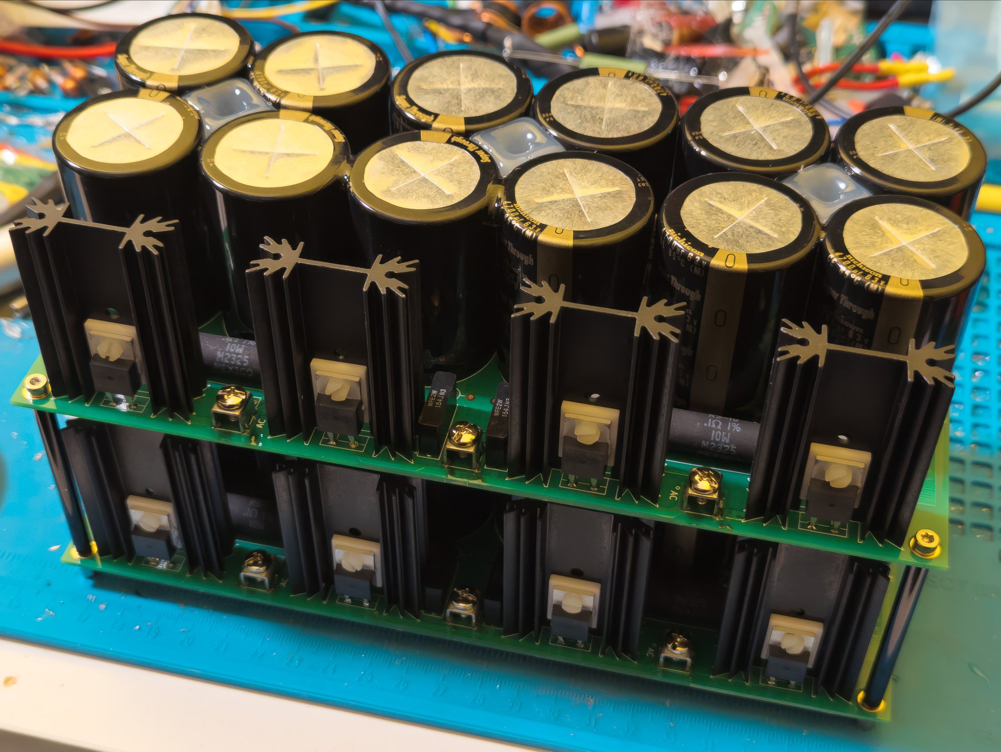
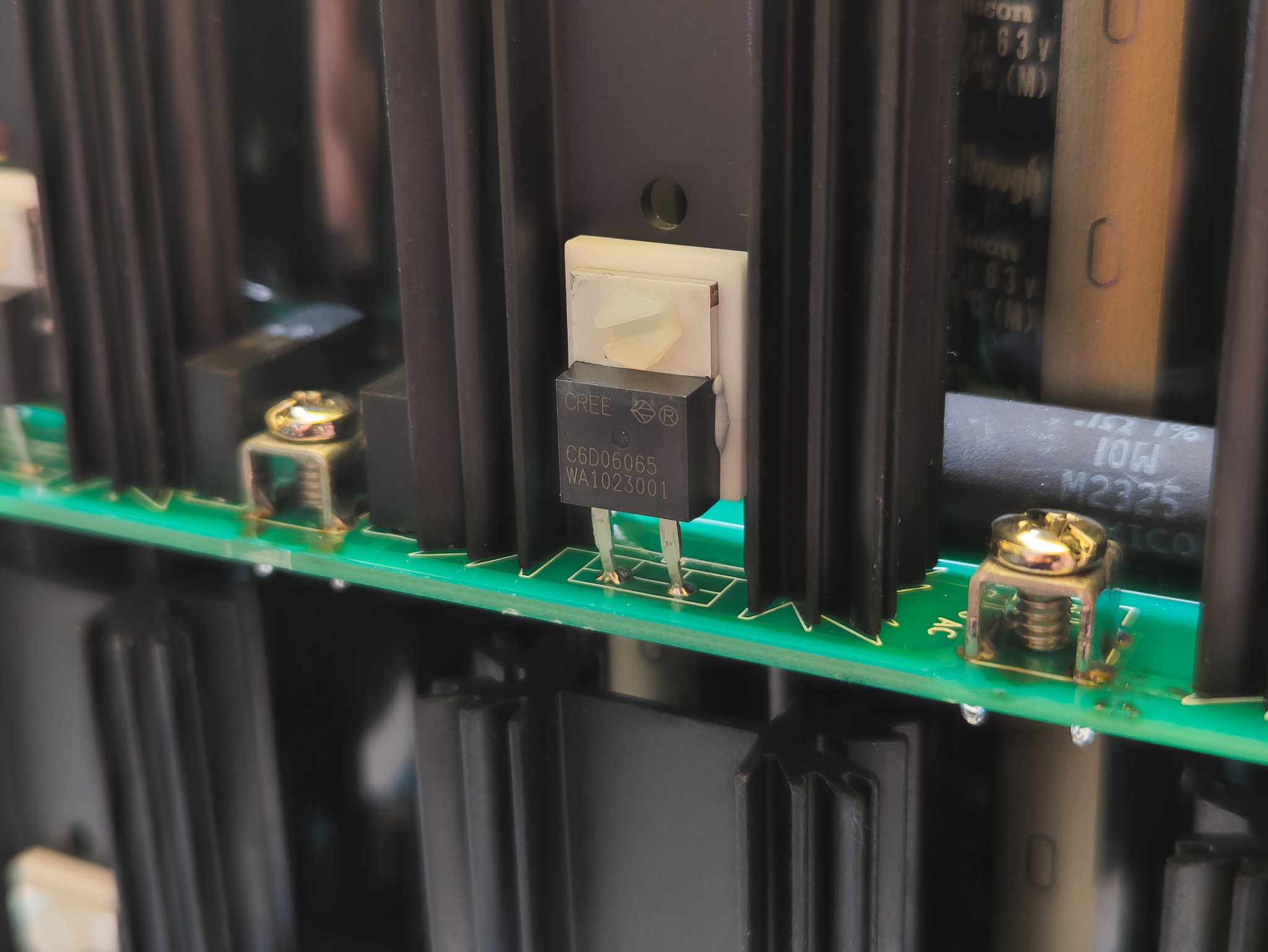
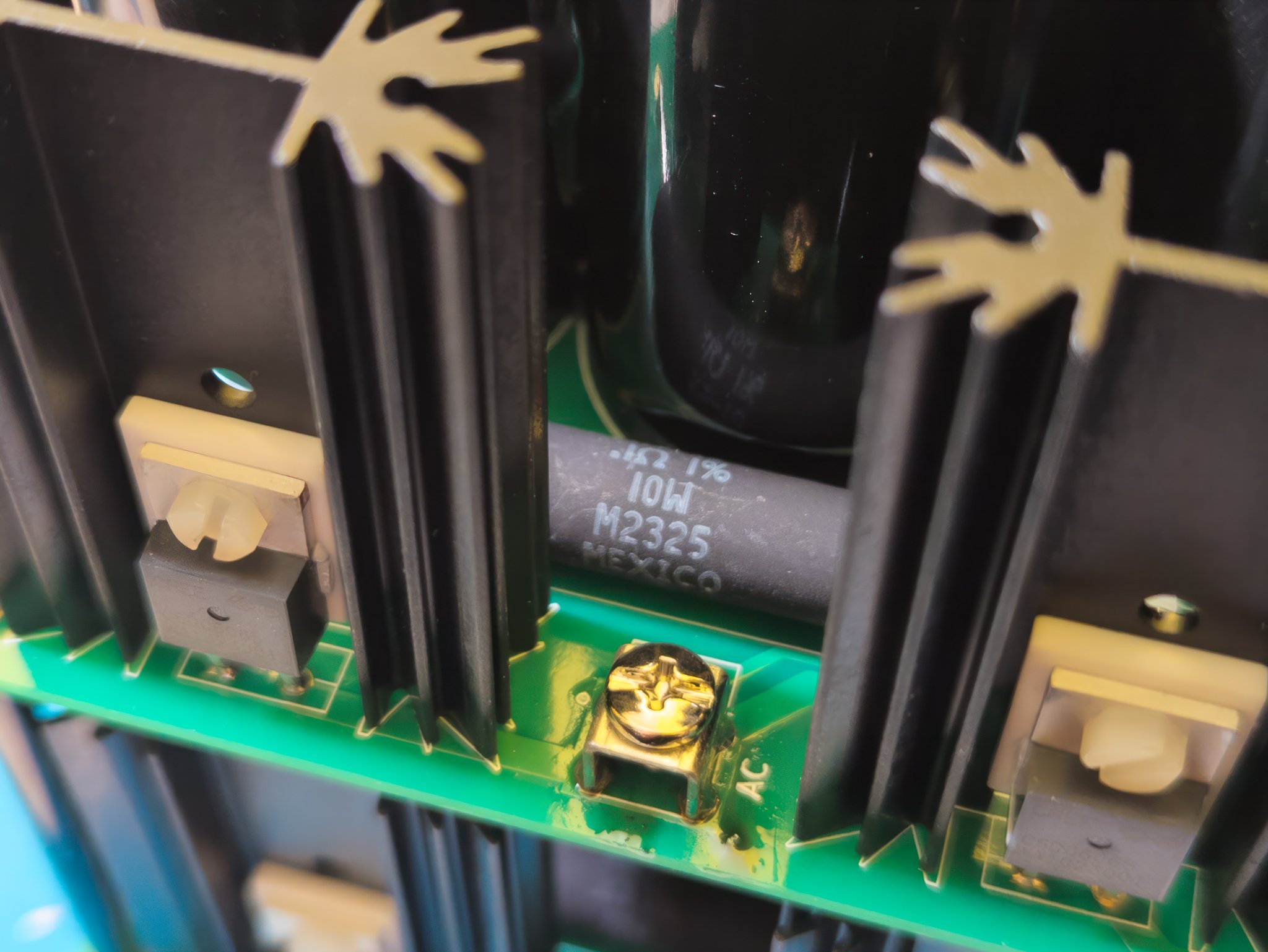
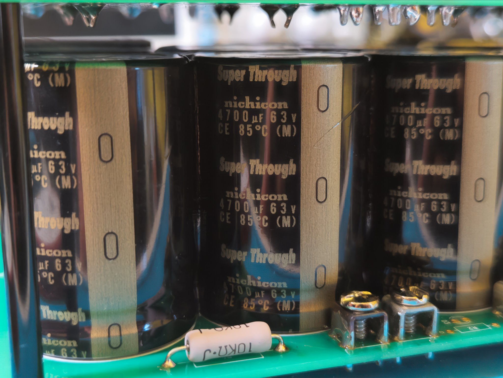
I've done some work on the power supplys for my new FSSA build this weekend...
- Home
- Amplifiers
- Solid State
- FSSA amplifier build thread with review
