Thanks Ludilu.
That's really good clarification.
Certainly lots of potential.
Will follow with interest.
That's really good clarification.
Certainly lots of potential.
Will follow with interest.
Member
Joined 2018
Thank you Speedysteve7-San
For cheering on this project. It's my pleasure.
Thanks, Ludwig-San

An unbalanced connection will connect the cold side terminal to GND. This connection has no problem.
On another hand, the Solidsate output circuit should connect like this...

The cold side output signal will be fed to GND through a low-impedance resistor. (shown in RED color)
This type of connection consumes so much power for termination. Now I'm thinking this does not make sense.
So I devised the following circuit for the differential output driver.

The simulated result shows the signal will be reproduced even if the target equipment's GND level has a differential potential voltage VG.
(This voltage VG should be inside of power rails)
Now I'm starting to design a new output driver circuit with this idea...
CyberPit
For cheering on this project. It's my pleasure.
The current design has 8ch analog output + one S/PDIF optical output. So, if you add a stereo DAC or Amplifier with S/PDIF you'll have total 10 outputs routed as of now.I have 10 channel requirement, but get around that by analogue XOs on the tweeter channels.
If there are plans for a 10 out Octavia, I'd be very interested.
Thanks, Ludwig-San
Ordinary transformer output can connect this way...I am not so familiar with the term "cold-side termination". Can you eloberate this?
An unbalanced connection will connect the cold side terminal to GND. This connection has no problem.
On another hand, the Solidsate output circuit should connect like this...
The cold side output signal will be fed to GND through a low-impedance resistor. (shown in RED color)
This type of connection consumes so much power for termination. Now I'm thinking this does not make sense.
So I devised the following circuit for the differential output driver.
The simulated result shows the signal will be reproduced even if the target equipment's GND level has a differential potential voltage VG.
(This voltage VG should be inside of power rails)
Now I'm starting to design a new output driver circuit with this idea...
CyberPit
Last edited:

Member
Joined 2018
A piece of good news comes after trial work...
I evaluated the previously posted differential driver circuit. It was not stable and noisy when connected to the ground potential sens line.
So I gave up sticking to the perfect differential behavior design. The compromised design as below works fine with differential RCA output or XLR Balanced output (Not at a time, you need to use only one connection method)

Non-Inverted output(RCA pin output) only works as differential output, but it's enough for actual use cases. If you connect only XLR, this circuit will work as a typical balanced output design. No need to operate the switch or change components, you just unplug the connector and then connect another type of connector.
Here's evaluated performance information
Remain Noise


Full-Bit Output Distortion


Best THD performance@-12dB FS

I hope someone evaluates this circuit more if possible.
I would like to start improving the schematic design.
CyberPit
I evaluated the previously posted differential driver circuit. It was not stable and noisy when connected to the ground potential sens line.
So I gave up sticking to the perfect differential behavior design. The compromised design as below works fine with differential RCA output or XLR Balanced output (Not at a time, you need to use only one connection method)
Non-Inverted output(RCA pin output) only works as differential output, but it's enough for actual use cases. If you connect only XLR, this circuit will work as a typical balanced output design. No need to operate the switch or change components, you just unplug the connector and then connect another type of connector.
Here's evaluated performance information
Remain Noise
Full-Bit Output Distortion
Best THD performance@-12dB FS
I hope someone evaluates this circuit more if possible.
I would like to start improving the schematic design.
CyberPit
Hi CyberPit-San,
thanks for the explaination. I get your point now.
Maybe one thought regarding the stability issue on your initial redesign.
When I started creating the simulation I was also thinking about moving the low pass filter at the output of the dac into the opamp design. This should also improve stability. The only downside would be that this would not affect the non differential output, but here we could leave the pads for the current filter.
Basically like this example from the datasheet :

BR Ludwig
thanks for the explaination. I get your point now.
Maybe one thought regarding the stability issue on your initial redesign.
When I started creating the simulation I was also thinking about moving the low pass filter at the output of the dac into the opamp design. This should also improve stability. The only downside would be that this would not affect the non differential output, but here we could leave the pads for the current filter.
Basically like this example from the datasheet :
BR Ludwig
Another approach that works doesn't require anything other than a resistor to match the impedance on the 'cold' leg to that of the 'hot'. Only the 'hot' is then driven with a signal. Max output with a PCM5102a would be 2.1V which is enough to drive the vast majority of amplifiers into clipping. No need for opamps or mute circuits, can then use the PCM5102a mutes.
Check the article on balanced below:
https://linea-research.co.uk/white-papers/
Check the article on balanced below:
https://linea-research.co.uk/white-papers/
Member
Joined 2018
SubSoniks-San, Ludwig-San,
Thanks for giving comments.
The True transformer-simulated design keeps the same output voltage in Balanced and Unbalanced connections.
But I wonder, it is not a big matter. Just decreasing the volume by -6dB in the balanced connection case. This is not a difficult thing.
Now, I'm starting the detailed design of the Differential/Balanced output driver circuit.
Considering AC performance lead me to decide the compromised version.
I try to re-design the full-balanced version circuit. But keeping audible Hi-Res bandwidth is very very difficult.
Here's an optimized frequency response version design.

A low-pass filter characteristic requires a very complicated design. A small balanced output difference remains after tuning the components. And it not be able to ignore.
And here's a compromised version AC simulation

This design has no problem even if the Hi-res audio bandwidth application. According to the performance and number of necessary components, this version circuit has great advantages compared to the previous one.
I guess, now I can start redesigning the OVtAVIA's output driver circuit.
CyberPit
Thanks for giving comments.
The True transformer-simulated design keeps the same output voltage in Balanced and Unbalanced connections.
But I wonder, it is not a big matter. Just decreasing the volume by -6dB in the balanced connection case. This is not a difficult thing.
Now, I'm starting the detailed design of the Differential/Balanced output driver circuit.
Considering AC performance lead me to decide the compromised version.
I try to re-design the full-balanced version circuit. But keeping audible Hi-Res bandwidth is very very difficult.
Here's an optimized frequency response version design.
A low-pass filter characteristic requires a very complicated design. A small balanced output difference remains after tuning the components. And it not be able to ignore.
And here's a compromised version AC simulation
This design has no problem even if the Hi-res audio bandwidth application. According to the performance and number of necessary components, this version circuit has great advantages compared to the previous one.
I guess, now I can start redesigning the OVtAVIA's output driver circuit.
CyberPit
Member
Joined 2018
I forgot to upload the balanced output mode simulation.

This design will be a Differential RCA-pin output = 2Vrms, XLR output = +12dBV = +14dBv maximum.
CyberPit
This design will be a Differential RCA-pin output = 2Vrms, XLR output = +12dBV = +14dBv maximum.
CyberPit
I guess the downside of this variant is that the balanced circuit will only reject common mode noise on the cable to the amp and not due to noise on the GND on the octavia. (See VP-VN with ground noise). I also wanted to play around in the simulation with the perfect differential design, but I didn't find the time to do so. Hopefully in the next couple of days.
At the moment I am analysing the PCB layout. From looking at the layout it is to expected that the performance differs between the channels. I still have to confirm that the channels I would rate the worst from the layout are actually meassuring the worst in real life.
I also want to measure crosstalk between the channels. Some channels look likely to be influenced by other channels (especially the ones with the long quad DAC connections). Lets see what the measurements will show.
Best Regards,
Ludwig
Member
Joined 2018
Thanks, Ludwig-San,
If we take the compromised version driver circuit. We should remove the Quad-DAC feature anyway.
But this also means less crosstalk chance in a new PCB layout.
We should compromise and get something good on this point... 🤔
CyberPit
If we take the compromised version driver circuit. We should remove the Quad-DAC feature anyway.
But this also means less crosstalk chance in a new PCB layout.
We should compromise and get something good on this point... 🤔
CyberPit
Hi CyperPit-San,
I think removing the Quad-Dac will help. I don't know how much interest there is for this feature.
The inner perfectionist in me does not want to settle with a compromised solution 😆 . I will try experiment a bit on the weekend.
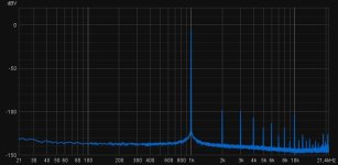
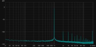
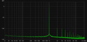
Here is an examples of crosstalk I measured today. I had a 1kHz signal on 32/33. One picture is without any other channels active, one with 10k on 40/41 and one with 20k on 40/41.
Regarding PCB layout. What was your reasoning behind goding for a 2 layer PCB? A 4 layer PCB is about 4 USD more expensive per board but offers much better capabilites for signal integrity and EMI. It also makes the routing easier in some regards. Maybe we should think about this too.
Best Regards,
Ludwig
I think removing the Quad-Dac will help. I don't know how much interest there is for this feature.
The inner perfectionist in me does not want to settle with a compromised solution 😆 . I will try experiment a bit on the weekend.
Here is an examples of crosstalk I measured today. I had a 1kHz signal on 32/33. One picture is without any other channels active, one with 10k on 40/41 and one with 20k on 40/41.
Regarding PCB layout. What was your reasoning behind goding for a 2 layer PCB? A 4 layer PCB is about 4 USD more expensive per board but offers much better capabilites for signal integrity and EMI. It also makes the routing easier in some regards. Maybe we should think about this too.
Best Regards,
Ludwig
Attachments
Member
Joined 2018
Hello LinuksGuru-San,
PCM1840 is not bad. From the point of view of Dynamic Range and DIstortion, plus input bandwidth filtering features, it costs 10% of the total board parts plus it requires 4 times balanced driver input buffers(i.e. OPA1632). It's gonna too much input balance-weighted design today. PCM1804 is not expensive but also requires two balanced drivers with antialiasing filters.
I guess those chips should apply to the J3 I2S/TDM Input Header's optional board.
2ch for MM pickup and the rest of 2ch for MC pickup, or totally full-balanced Phono-Amp will be interesting.(Of course Flat head Amp and DSP RIAA-EQ)
Just an idea but it's my pleasure. 😎
CyberPit
Last edited:
Hi, CyberPit-San, sorry, I didn't understood clearly, so both 1840 and 1804 will fit J3 I2S/TDM Input Header's optional board, or only 1804? I'm looking for best possible ADC option, 1804 will not fit for me. Thanks.
Member
Joined 2018
Hi LinuksGuru-San,
J3 I2S/TDM Header can support up to 16ch TDM ADC. (2ch/4ch/8ch/16ch)
One of my friends told me, he's thinking about Quadraphonc Encoder & Decorder combined with OCTAVIA board.
PCM1840 will be an excellent choice for this kind of application.
CyberPit
J3 I2S/TDM Header can support up to 16ch TDM ADC. (2ch/4ch/8ch/16ch)
One of my friends told me, he's thinking about Quadraphonc Encoder & Decorder combined with OCTAVIA board.
PCM1840 will be an excellent choice for this kind of application.
CyberPit
Heads up re the PCM1840, there is a high pass filter at 8Hz/48KHz which scales with sample rate.
Member
Joined 2018
Hello guys, Here's the new version 0.3 schematic circuit diagram of FreeDSP OVTAVIA.
Due to the output circuit change, the quad DAC mode was deleted.
The changed points are...

The next step is PCB design.
The board will be changed to four layers PCB to increase the audio performance more.
CyberPit
Due to the output circuit change, the quad DAC mode was deleted.
The changed points are...
- A low distortion new differential RCA-pin output circuit.
- Double XLR output level. (4V RMS)
- Sync start/stop of -5V power rail with +5V rail.
- decrease cut-off freq of PCM5102A post-LPF.
- Fixed previous issues.
The next step is PCB design.
The board will be changed to four layers PCB to increase the audio performance more.
CyberPit
Attachments
Hi CyberPit,
I was trying to do some simulations and also rebuild your compromised circuit, but somehow I cannot get the same results. My VP is not a sine, i jumps from -4.4 to +4.4V which I would kind of expect since there is no feedback. What am I missing here?
Also, I read quite a bit about mixed signal layout and I often found that it is better to have one entire ground plane instead of separate split ground planes. What is your opinion on that?
Ludwig
Member
Joined 2018
Hi Ludilu,
Here's a subcircuit model that is used in MC12.
Maybe useful...
A pure separate-ground idea is not easy with common powered circuits. Using an output transformer design is the only way to realize that concept. So I'm planning star-like layout design topologies. The cross point will be a power of DACs. The output signals will return with each balanced pair or ground line and finally, it will back to the signal source device. If the power rails are de-coupled and stabilized very well, the crosstalk level will be the sum of the device's internal limits and stray capacitance coupling level. Just think about the output current going to the load device and returns. Which path will be used? That is a design starting point.
CyberPit
Attachments
Last edited:
Hi CyberPit-San,
thanks for the sub circuit. I'll have a look this evening.
Regarding the ground planes. With separate I mean the star layout. I read that one common ground is better than the star layout if you can separate digital signals from analog ones, which should be the case here (See the book Electromagnetic Compatibility Engineering by Henry W Ott; there is a chapter about mixed signal PCB layout)
BR Ludwig
- Home
- Source & Line
- Digital Line Level
- FreeDSP OCTAVIA