Later I continued searching for more info. I found JeffYoung "Long skinny builders" thread.
Long skinny builders thread
Attached file DIY-J2-LTP-current.pdf (Determining the LTP current “sweet spot” for a DIY J2 clone.)
Interesting read of how Jeff found his CCS "sweet spot" of 8.5mA.
I guess 7-10mA is still okey spot and ever higher.
Great thank you for pointing this article, really helpful to understand the circuit.
> Nelson himself have already answer that question here at post 1130
He was talking about the resistor for the current source (top) MOSFET.
I was talking about the bottom one.
> I want to make a version with irfp150 up and down first.
Cheers,
Patrick
He was talking about the resistor for the current source (top) MOSFET.
I was talking about the bottom one.
> I want to make a version with irfp150 up and down first.
Cheers,
Patrick
This is good research, thanks for sharing. The only real data point I've been operating with came from Nelson in an email, which suggested that "common wisdom" is something like 10% off Idss. Noting that with diff pairs that other things like the resistor loading off the Drain are also considerations.
I think the lesson is that every scenario is going to be a little different, and you're wise to be doing the spice modeling and other tests.
Personally, I also have to think that there's some wiggle room in all of this. One thing I can say with certainty is that I followed the above logic with my recent AJSS build and had outstanding results.
Good!
Nelson is a valuable source of information when we talk about First Watt amplifiers. 😀
Someday J2 production ceases and we will have official info to play.
And even expansive JFETs wil not stop us. 😀😀😀


> Nelson himself have already answer that question here at post 1130
He was talking about the resistor for the current source (top) MOSFET.
I was talking about the bottom one.
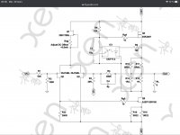
I have a 2k trim pot in the place of r33 on your schematic. It is set at 1k1 in my simulation and everything is looking fine. Is that what you were talking about? Anything else I should take a look at?
Hubert
Attachments
I'm about to populate the EUVL designed PCB's from post #1393.
I'm going with IRFP240's for Q4. Semisouths are from Papa via CodyT (Thanks again gents!!!!)
I plan to start with sockets in R33 position to adjust if needed.
What I can't seem to find is how to deal with Rdg...
What should the initial setting of the Rdg pot be when building? I got a 500R pot.
Can anyone help help me understand this better?
"Rdg - Adjust DC Offset ~8.5mA"
DC Offset at speaker terminals after amp is warmed up?
Best way to measure 8.5mA in circuit?
> "Rdg - Adjust DC Offset ~8.5mA"
This means that you can work out the rough value of Rdg off board by measuring the current through the current source.
For example with a multimeter.
> DC Offset at speaker terminals after amp is warmed up?
Yes, after presetting the Rdg as described above.
> Best way to measure 8.5mA in circuit?
If you have to do this in circuit, you should follow the schematics and use 300R for R33.
Then, without any of the power devices installed, short both inputs to Gnd.
Measure the voltage across R33 and divide that by 300R to get current.
But this is just a rough set-up to get you roughly there.
The exact setting varies with the Vgs of your power devices.
You still need to fine trim after fitting in the power devices and warm up to steady state.
Patrick
>> "Rdg - Adjust DC Offset ~8.5mA"
>This means that you can work out the rough value of Rdg off board by measuring the current through the current source.
For example with a multimeter.
I've never done this. is there a post, article, diagram, or "how to" for this?
>This means that you can work out the rough value of Rdg off board by measuring the current through the current source.
For example with a multimeter.
I've never done this. is there a post, article, diagram, or "how to" for this?
I'm building the same amp, except I'm using 2SK3497 for CCS.
For Rdg, I adjust the voltage across 300 ohm R33 to 2.55 vdc with inputs IN+ and IN- to ground.
Then with the power devices installed, Rdg adjust for DC offset across speaker terminals. as a fine adjust after thermal stability.
I noticed in the schematic the gate resistors for the power devices also have a designation that seems to be something the builder should adjust. Is this to tune the output devices to equal current flow?
@elwood625, I won't comment about the gate resistors here but generally the gate resistors are there to prevent oscillation. To tune the output devices to achieve equal current flow, you might refer to the UDNeSS Revisions pdf which speaks to measuring current sharing and adjusting for equal sharing:
Post 89
The respective current contribution of Q4 and Q5 were then measured; and were found to deviate from to 1:1 as intended. As a result, the values of R11~R14 were adjusted to be 0R34:0R56. This can be verified by measuring the AC voltage across R15. When the output is 8V p-p into 8R, the AC voltage across R15 should be 250mV p-p. These are now set to be the new default values, but might still vary in real life for different MOSFET batches with different transconductances. The ratio does not have to be exact, and 10% variation will have little impact on resulting distortion spectrum.
Gate resistors are fixed, no adjustments.
Increasing R6 will allow you to increase bias of the current source, vice versa.
So R6 & Rdg are the only two adjustments you need to make.
Unless of course you wish to play with current sharing & distortion spectrum.
FirstWatt J2
Patrick
Increasing R6 will allow you to increase bias of the current source, vice versa.
So R6 & Rdg are the only two adjustments you need to make.
Unless of course you wish to play with current sharing & distortion spectrum.
FirstWatt J2
Patrick
No need to change R11,14 unless you have a distortion analyser, and know what you are doing with it.
Patrick
Patrick
Hi Patrick -
Making a change to R6, will this change the current flow through both devices or just Q4?
To measure the current through each device:
For Q4, measure the voltage drop across R11-R12 to calculate current?
For Q5, measure the voltage drop across R15-R16 to calculate current?
Bill
Making a change to R6, will this change the current flow through both devices or just Q4?
To measure the current through each device:
For Q4, measure the voltage drop across R11-R12 to calculate current?
For Q5, measure the voltage drop across R15-R16 to calculate current?
Bill
Only Q4. So if you change R6, youneed to readjust DC offset.
> So measure the current through each device:
> For Q4, measure the voltage drop across R11-R12 to calculate current?
> For Q5, measure the voltage drop across R15-R16 to calculate current?
Yes, but you only need to check for either Q4 or Q5.
Once your DC offset is zero, Id Q5 automatically equals Q4.
Patrick
Is there a target current flow to set R6 or is the R6 adjustment to get zero offset and 8.5mA across R33?
Bill
Bill
Why not just build using the published schematics first and see what current you get through Q4, Q5 ?
Patrick
Patrick
- Home
- Amplifiers
- Pass Labs
- FirstWatt J2