ok, resistance at drain? I see only Rs at the gates or the P1 at source.
Understanding circuits is not my best.
Understanding circuits is not my best.
if you want to stay out of public, send me your sch to zenmodiyaudio^gmail.com, and I'll give you specific answer
Hi Aleksandar, do you see a danger of thermal runaway, when Carsten replaces the SS with IRFP240. Should he choose higher source resistors?
just for variety sake , find enclosed few files
few years ago , one of Greedy Boyz contacted me for pcbs - Pa gratiously gave him all semis for J2 , same as nudge to pass me an order to make him set of pcbs
so , there it is , crudest and fastest and simplest I could do at moment , without too much things added ...... didn't go for miniaturization simply because SSouths need to be spread anyway ....... so - one sided pcb (that's why few shorties), use thick copper
FE made with 2SJ109 , use whatever you have in drawer (it's easier to put two 2SJ74 in pinout of 2SJ109 , than the other way 🙂 )
take Patrick's values
feel free to use it for your own pleasure
edit: in case of using IRFP outputs - change that trimpot to 1K or so ... or even better - cut trimpot trace and insert 680R in line
Digging up an old posting. I've got the PCB's from this post and I'm working on schematic values to use with my SemiSouth gift pair from Papa. (Thx again!)
According to ZM's notes/schematics- I should take some values from EVUL's schematic. Of course, each schematic is not identical, so there's some guessing involved for a novice fearless amp builder.
Thanks for the help!
Q-
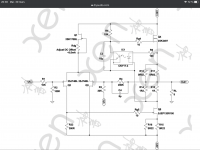
Resistor values using IRFP240 for Q3. Q4 would be a Semis.
R8 schematic says 0. Jumper?
R10 schematic sys 0. Jumper?
R11- 10K
R15- 0R82
R16-1R2
R17- 0R22
R18- 0R82
R19- 1R
R20- 0R22
ZM notes say change trimpot to 1K. I think this means R6. Or cut trace and use 680R. The trace going to OC1?
Digging up an old posting. I've got the PCB's from this post and I'm working on schematic values to use with my SemiSouth gift pair from Papa. (Thx again!)
According to ZM's notes/schematics- I should take some values from EVUL's schematic. Of course, each schematic is not identical, so there's some guessing involved for a novice fearless amp builder.
Thanks for the help!
Q-
Resistor values using IRFP240 for Q3. Q4 would be a Semis.
R8 schematic says 0. Jumper?
R10 schematic sys 0. Jumper?
R11- 10K
R15- 0R82
R16-1R2
R17- 0R22
R18- 0R82
R19- 1R
R20- 0R22
ZM notes say change trimpot to 1K. I think this means R6. Or cut trace and use 680R. The trace going to OC1?
0 (or 0R) means jumper
R6 is sole trimpot on pcb
if you have difficulties to grasp how to add 510R in series with 500R trimpot, then change trimpot to 1K
I also appreciate any insight into values used for EVUL pcb v2 09/19. Unsure whether I will use IRFP 240 or 150 and my pair of R120s. Taking my time with this and not rushing as the recent Aleph J build has me content for now.
I was scouring pages to try and find consensus value for Rdg with either fixed value or trimmer.
Have determined BL grade at 6-8 Idss for the upper 170 and lower 2x J74 at GR with Idss 4mA.
I was scouring pages to try and find consensus value for Rdg with either fixed value or trimmer.
Have determined BL grade at 6-8 Idss for the upper 170 and lower 2x J74 at GR with Idss 4mA.
0 (or 0R) means jumper
R6 is sole trimpot on pcb
if you have difficulties to grasp how to add 510R in series with 500R trimpot, then change trimpot to 1K
Zen Mod, Thanks! It's clear to me from your answers.
I also appreciate any insight into values used for EVUL pcb v2 09/19. Unsure whether I will use IRFP 240 or 150 and my pair of R120s. Taking my time with this and not rushing as the recent Aleph J build has me content for now.
I was scouring pages to try and find consensus value for Rdg with either fixed value or trimmer.
Have determined BL grade at 6-8 Idss for the upper 170 and lower 2x J74 at GR with Idss 4mA.
I’m at the same place as you are. I have began a J2 project with evul pcb v2 since I now have a R120 pair 😀
I’ve decided to go with the irfp150 since I want to make a version with irfp150 up and down first. Like Zenmod have done in his Babelfish J2. Just want to be sure that the circuit is behaving properly before putting my precious semisouth into it. I have chose to take the resistors values from Zenmod schematic for the output transistors.
As for the front end, my k170 are 8.5ma idss and the j74 are 9.2ma idss. Evul specify BL grade for the j74. I think rdg is not needed if your front end transistors are properly chosen and if you replace r33 with a trimpot. I’m not sure about the exact idss / idss ratio that is ideal. It would be great if someone more knowledgeable could help with that!
Hubert
Attachments
Yes I have seen your post about this. I have tried to keep the same ratio as you have in your Aleph J2 front end. Thank you Cody!
BL , matched and you're good
though, Papa posted interesting things here, making our (read us Toshibascavengers) miserable Lives somewhat easier:
Beyond the J Fringe
though, Papa posted interesting things here, making our (read us Toshibascavengers) miserable Lives somewhat easier:
Beyond the J Fringe
Hierarchical ground is where you sort the connections by level of dirt -
transformer on the bottom, input and feedback grounds on the top.
😎
The XLR shield goes to its designation on the AMP PCB. I used a slight twist of + and - input signal wires and included the shield bare litz (multi-strand) wire in that twist as well. The ground-lift resistor must be removed (if previously used with RCA's, i.e. with amp wired to accept the single-ended input, which was how I used the amp initially).
It is important that the shield (bare) wire does not touch the chassis; the chassis and the amplifier ground are separated by the CL60, which in this case provides a 10 ohms difference between these two potentials.
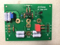
The speaker negative (return) should not go to the amp PCB -> it should go to the power supply PCB. The power supply PCB does not really have a ground segregation provision(s); the best you could do is to look at the second photo I attached. I used the X4 ground connection on the PS PCB for an additional decoupling capacitor....; however, the X4 (visible on the photo, only just <- left-hand side) is an even better point to return the signal ground from the AMP PCB.
NOTE: The first photo is an old photo - it shows the speaker return going back to the AMP PCB...
Aleph J needs two power supplies; using the separate power supplies will bring an additional level of benefits to its separation of sound (the perceived left-right, and top-bottom extension).
Edit: The latest photo attached.
I saw this Nelson's post last night while browsing...it's from 2016... I wish I'd seen it just before I started my Aleph J build... would've saved me a lot of time.
Getting the returns sorted out correctly is very important, especially with a single PS PCB. There's a HUGE difference in sound between good and bad - stereo separation and bass ground bounce (boomy bass) benefit the most.
> I’ve decided to go with the irfp150 since I want to make a version with irfp150 up and down first.
> I have chose to take the resistors values from Zenmod schematic
The SJEP has a Vgs of ~1V at bias. The IRFP150 ~4.5V.
Since you are following ZM schematics, I am sure he'll guide you to get round that.
😉
Cheers,
Patrick
> I have chose to take the resistors values from Zenmod schematic
The SJEP has a Vgs of ~1V at bias. The IRFP150 ~4.5V.
Since you are following ZM schematics, I am sure he'll guide you to get round that.
😉
Cheers,
Patrick
> Unsure whether I will use IRFP 240 or 150 and my pair of R120s.
Have you tried the search function for this thread ?
FirstWatt J2
> I was scouring pages to try and find consensus value for Rdg with either fixed value or trimmer.
> Have determined BL grade at 6-8 Idss for the upper 170
It depends on the Idss of your 2SK170.
FirstWatt J2
The schematics I posted says that you need a Rdg to adjust bias to ~8.5mA.
I guess 6~8mA Idss will not get you that, whatever the value of Rdg ?
Patrick
As for the front end, my k170 are 8.5ma idss and the j74 are 9.2ma idss. Evul specify BL grade for the j74. I think rdg is not needed if your front end transistors are properly chosen and if you replace r33 with a trimpot. I’m not sure about the exact idss / idss ratio that is ideal. It would be great if someone more knowledgeable could help with that!
Hubert
I have been told 90% of LTP Idss
I am also gathering information on J2 and try to fill spaces in knowledge.
Some thinking out loud. Please correct me if I am wrong.
According to Patrick schematic from post 1274 his LTP CCS is 8.5mA:
FirstWatt J2
LTP will be biased by that current.
8.5mA CCS will be split to each input JFET. That is about 4.25mA for two.
Although as I understand J2 means all JFETs are doubled and this schematic cut every part to "J1".
If we back to doubled LTP JFETs (4 pcs of SJ74), 8.5mA CCS will split to about 2.125mA for each input JFET.
Does doubling input JFET pairs help?
I took Patrick ltspice files from post 1253 and 1255 of J2 with 1 input JFET pair and 2 input JFET pairs and unpack all files in the same folder.
Rail is 24V
J2 with 1 pair of input JFETs shows THD of 0.032075% with CCS 8.84 mA
Each LTP JFET dissipates about 100mW.
Then I open a J2 file with 2 input JFET pairs.
For testing purposes to have the same input CCS I cut the second 2SK170 and change R110 to 300 Ohm.
J2 with 2 pairs of input JFETs shows THD of 0.021457% with CCS 8.84 mA
Each LTP JFET dissipates about 49.5mW.
0.010618% THD difference.. but I guess LTP is even more safe and thermally stable that way.
That's just a simulation.
Back to CCS current.
Post 695 Nelson said he have it at about 8mA.
If you are referring to the input bias CCS, then that does sound like
a bit much. I run about 8 mA.
😎
Later I continued searching for more info. I found JeffYoung "Long skinny builders" thread.
Long skinny builders thread
Attached file DIY-J2-LTP-current.pdf (Determining the LTP current “sweet spot” for a DIY J2 clone.)
Interesting read of how Jeff found his CCS "sweet spot" of 8.5mA.
I guess 7-10mA is still okey spot and ever higher.
About CCS Idss:
From First Watt B1 article ".. The Idss is simply the current that flows through the JFET when the Gate and Source are grounded and +10 volts or so is applied to the Drain. .."
So Idss = current that flows when Gate and Source pins attached and about ~10V applied. (also datasheet values was tested on the same voltage)
On 24V rail it will be a little bit more, about 0.15mA
For 8.5mA CCS of two 2SK170 you need each JFET to be about 4.25 mA Idss or sum of different values.
That matching only needed for the clone of original J2 without a trim pot like Patrick did.
About LTP Idss:
I don't know the required Idss formula for this part.
Logically LTP JFETs should have Idss no less than current applied to it but will feel more comfortable being higher..
My guess for classic J2 would be LTP JFET Idss should be 4 times higher than current applied to it.
That means about the same Idss for each of 2SK170 and 2SJ74 JFETs.
"Thinking out loud" mode off.
This is good research, thanks for sharing. The only real data point I've been operating with came from Nelson in an email, which suggested that "common wisdom" is something like 10% off Idss. Noting that with diff pairs that other things like the resistor loading off the Drain are also considerations.
I think the lesson is that every scenario is going to be a little different, and you're wise to be doing the spice modeling and other tests.
Personally, I also have to think that there's some wiggle room in all of this. One thing I can say with certainty is that I followed the above logic with my recent AJSS build and had outstanding results.
> I’ve decided to go with the irfp150 since I want to make a version with irfp150 up and down first.
> I have chose to take the resistors values from Zenmod schematic
The SJEP has a Vgs of ~1V at bias. The IRFP150 ~4.5V.
Since you are following ZM schematics, I am sure he'll guide you to get round that.
Nelson himself have already answer that question here at post 1130 : FirstWatt J2
My spice simulation seem to confirm that as well.
Attachments

- Home
- Amplifiers
- Pass Labs
- FirstWatt J2