Sorry for dump question.... when Nelson says -Vgs is greater is it greater in pos or in neg axis direction?The -Vgs of the SIT is greater than that of the P channel part, and the resistance between the Sources is chosen for the desired bias.
probably meaning in absolute value
anyhow, everything explained in https://www.diyaudio.com/community/threads/redneck-zm-defisit-def-biasing.373938/
anyhow, everything explained in https://www.diyaudio.com/community/threads/redneck-zm-defisit-def-biasing.373938/
Can anyone explain these pieces on the SIT-5 Owner Manual:
These appears to be an inconsistency here. How can we have both:This arrangement is unique in that the SIT is given a single-
ended Class A bias current by the P channel Mosfet which is allowed to make a smaller
contribution to the output, typically about 20%. This is seen on the right hand side of the
schematic where the output goes through two sets of power resistors and capacitors.
By adjusting the ratios of these power resistors, through the two output capacitors, we can
trim the load line of the SIT so that it dominates the output character, adds a little to the output
power, but mostly gives a consistent character across a population of SIT devices.
- P channel Mosfet which is allowed to make a smaller contribution to the output, typically about 20%.
- By adjusting the ratios of these power resistors, through the two output capacitors, we can trim the load line of the SIT so that it dominates the output character, adds a little to the output power.
relax Bro, you know that Pa is, most often than not, making OMs with copy-paste procedure ( as is logical)
so, what's few inconsistencies between friends?

(I remember reading X5 SM, where figures given for setting Iq and whatnot, are resulting in somewhere near 2KW of heat; darn tech needs to have brain engaged, don't you think..... )
so, what's few inconsistencies between friends?
(I remember reading X5 SM, where figures given for setting Iq and whatnot, are resulting in somewhere near 2KW of heat; darn tech needs to have brain engaged, don't you think..... )

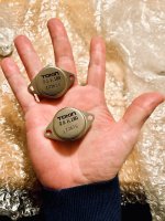

Holy Schade, these things are huge and heavy!
Sorry… man child! Can’t let that one fly unnoticed!
I call it "middle earth" ...... :--))"no need to spice
put two series resistors of (say) 10K in between GND and other rail; mid point is amp's reference point; call it whatever you want
....... "
For the P-mosfet, the 'standard' thought is to the very macho IXTN40P50P and similar. Then you need the source resistor to create the benign Vgs bias.
But what about another legacy P-mosfet?
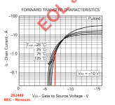
The 2SJ447 (NEC, lastly Renesas, EOL) has Vgs of nearly 7 volt at 1.5Amp. [I use it in a HV shunt]. The idea is that it allows a mucho smaller Rs, maybe zero. OK, the Vds max isn't that high, but that is not important here. The source resistance is not as low as the IXYS stuff though (3,5S/<0.8Ω-on vs 38S/>0.23Ω-pulsed). But the latter can be solved.
Ah. The Cero SIT-OM amplifier is born.
Paralleling for more than the little <6Amp should be possible. Because the transistor has a positive tempco, a small Rs of say 0.1Ω on each would be beneficient.
Of course, first look at the curse: the harmonics. . . .
But what about another legacy P-mosfet?
The 2SJ447 (NEC, lastly Renesas, EOL) has Vgs of nearly 7 volt at 1.5Amp. [I use it in a HV shunt]. The idea is that it allows a mucho smaller Rs, maybe zero. OK, the Vds max isn't that high, but that is not important here. The source resistance is not as low as the IXYS stuff though (3,5S/<0.8Ω-on vs 38S/>0.23Ω-pulsed). But the latter can be solved.
Ah. The Cero SIT-OM amplifier is born.
Paralleling for more than the little <6Amp should be possible. Because the transistor has a positive tempco, a small Rs of say 0.1Ω on each would be beneficient.
Of course, first look at the curse: the harmonics. . . .
Attachments
Then you will get mucho mos sound.The idea is that it allows a mucho smaller Rs
I'ld guess so too. But the internal resistance being high in comparison might reduce that effect.
2SK182ES sources:
Does anyone have recent experiences purchasing 2SK182ES SITs. I previously (several years ago) purchased some from Wattenabe on EBay.
Does anyone have recent experiences purchasing 2SK182ES SITs. I previously (several years ago) purchased some from Wattenabe on EBay.
I just sent a message, we will see!I just bought two 2SK182ES from pras1170. I believe there are still some available. I ordered January 10 and they came in the mail today. Lunar New Year is coming up, so things will probably be slower.
Russellc
Iirc ZM shown in the past in one of his threads (with an amp where square law os is implied and sit) that thf51 behaved better with 4r and k182es with 8r as load.
Also, the THF-51S is rated for 400 watts maximum dissipation while the 2SK182ES is rated for 500 watts. This gives the 2SK182ES an advantage when trying to run the SIT at higher power. For example, at 180 watts dissipated, that would be 45% of the limit for the THF-51S, but only 36% for the 2SK182ES.
Well I didn’t take that into account.
I went up to 100w dissipation, didn’t dare more on the sit because of the small heatsinks that I have for now.
What thermal interfacing are you using for 180w of dissipation?
At this dissipation level you can probably set the lower mosfet as a ccs and still get good performance at 4r.
What is the maximum dissipation that the bravest heart around went with these sits?
Up and running. Still might need some "tuning".

- Home
- Amplifiers
- Pass Labs
- First Watt SIT5