
Now the link for the SIT-5 on the First Watt page is active-
https://www.firstwatt.com/product/sit-5/
But when you download the manual, you get still the truncated version. ....
What a pity!
https://www.firstwatt.com/product/sit-5/
But when you download the manual, you get still the truncated version. ....
What a pity!

Thanks!
So no cascode feedback on the fe of this one.
Waiting for some heatsinks worthy of sit5 then probably will order the pch pucks too.
I am playing with a similar os but without square law.
I seen that adding square law helps at 4r to decrease a bit the 3rd hd and increase 2nd hd giving a more similar thd profile like the one you get at 8r.
I asked Nelson once why he gave up cascade feedback and he answered that there were some drawbacks.
But do you have any idea why these two resistors from j-fet out to j-fet in in series? Wherefore?
One thing could be to get the j-fet input at half the rail voltage, but why two and how to organize gain in this way?
Hu,Hu....
But do you have any idea why these two resistors from j-fet out to j-fet in in series? Wherefore?
One thing could be to get the j-fet input at half the rail voltage, but why two and how to organize gain in this way?
Hu,Hu....
that's simplified
of course that gate shunt resistor is referenced to mid rail
of course that NFB is referenced to same potential
it's just that circuit establishing that potential is left out
of course that gate shunt resistor is referenced to mid rail
of course that NFB is referenced to same potential
it's just that circuit establishing that potential is left out
I will spice!
no need to spice
put two series resistors of (say) 10K in between GND and other rail; mid point is amp's reference point; call it whatever you want
put (say) 100uF across 10K resistor at GND side
connect in gate shunt resistor to ref pint, connect shunt NFB resistor to ref point
you have it
now delete first 3 lines of this post, and you have drawing in OM

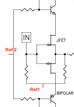
So, in this I added a Ref2 (the common central zero signal as you like it for the cascode device) and Ref1 the common for the input bias and the feedback zero.
Imho the two might combine. And have a shared cap to ground; but maybe the same cap also to the V-. (just to balance; it depends on the requirements for a 'slow start' as it might influence the DC point even though that inherent shift is not seen by output)
Imho the two might combine. And have a shared cap to ground; but maybe the same cap also to the V-. (just to balance; it depends on the requirements for a 'slow start' as it might influence the DC point even though that inherent shift is not seen by output)
Attachments
Always intrigued by what Papa comes up with, I've been following along with this thread. One point that doesn't seem to have been addressed yet, is the biasing at the Pfet's gate. Could it be as simple as a battery in series with the gate? It doesn't allow for fine tune adjustment of the bias and instead would rely on careful matching of the output devices and degeneration resistor. But it's super simple and eschews any problems with feedback or power supply noise that might come with other biasing schemes. Something like this...

Big thanks Aleksandar! Works!no need to spice
put two series resistors of (say) 10K in between GND and other rail; mid point is amp's reference point; call it whatever you want
put (say) 100uF across 10K resistor at GND side
connect in gate shunt resistor to ref pint, connect shunt NFB resistor to ref point
you have it
now delete first 3 lines of this post, and you have drawing in OM
Ah ok, I wasn't aware the SIT's needed a larger -VGS than the mosfet. I haven't messed around with SITs and was more focused on the topology. While the battery bias might have nothing to do with the SIT-5, could it be a viable solution for a DEF pairing with lower -VGS parts such as the IXYS depletion mode devices?
It depends on the exact SIT and it depends on the exact P MOSFET. The various combinations of higher and lower Vgs of the N vs P have been discussed in the DEF thread(s) and how to balance each situation.
If you are trying to use a large population if SITs in a production amplifier, then DEF is very time consuming to implement. Every amplifier has to be tweaked to balance the bias of the SIT against the P FET.
I think that the SIT 5 is intended to allow a widely varied population of SITs to be used in a particular circuit and no tweaking of each individual amplifier is required.
If there is tweaking, it could be accomplished by characterizing the SITs and characterizing the P MOSFETs and choosing the 2 resistors before building the amplifier. Make a kit that is SIT, PFET and 2 resistors. At the factory, just pull the kit and populate the OS. Then the amp goes to test and burn-in.
That is just my guess from reading the SIT5 manual and comparing the SIT5 circuit to the DEF circuit.
For the OS, the difference between SIT3 and SIT5 is 2 resistors and 1 capacitor. Just my thoughts.
- Home
- Amplifiers
- Pass Labs
- First Watt SIT5