well , good enough as detailed schematic .........
which smiley goes here .......... ....... or
which smiley goes here ..........
....... or The insert at bottom right is the F5 of course.
The bigger one is the F7. Too many parts? But it *works*. Whaddya want?

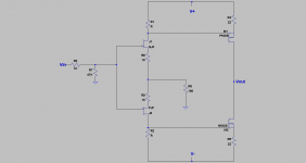
I cannot tell for sure from the photo, but based on the green wires from the channel PCBs to the power supply and the power supply traces it looks like the power supplies do not float w.r.t. ground.
The position of the power resistor near the output FET on the V+ rail puzzles me a bit. It suggests that the "extra resistor" that facilitates positive feedback might be between the output and the +rail FET and that none of my schematics are correct.
The resistors in the vicinity of the JFETs make sense for the various feedback schemes and for controlling the -3dB rolloff frequency.
It looks rather CCRC... but I might be wrong and ZM right 😕...CRCC supply...

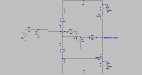
Experimenting with +ve feedback in diyF5
The front end of diyBA-3 [BA-3 FE] power amp may be used to understand the effect of positive feedback on the performance of a diyF5. Here's an explanation.
1. The left view is a simplified schematic of BA-3 FE.
2. The pot in the parent interconnecting the JFET sources was removed.
3. This is a low power circuit which may then be used to assemble the circuits advocated by lhquam and pr.
4. The emphasis is to initially practice a low instead of a high power amp, and get a feel for the systems' reaction.
The BA-3 FE simplified schematic is then modified by adding the circuit elements which are enclosed in parentheses as follows:
1. R11 = 500 Ohms to make it a mini diyF5 having a closed loop voltage gain =6.
2. Each of the 22 Ohm source resistors of the power Mosfets; is shunted with a 1,000uF electrolytic capacitor. The DC stability of the Mosfets is preserved, and the AC gain of the Mosfets is increased to look/be like that in the concept schematic of diyF7.
3. The fixed resistor R6 = 100 Ohm in the parent is replaced with a variable 100 Ohm.
4. The wiper of R6 is the point used to inject positive feedback via the added resistor R10 = 10 K to the joined gates of the JFETs. The article by Mr. Pass on F7 suggests that diyF5 is agreeable to accept some level of positive feedback.
Testing is done as follows:
1. Vi = 1.5 Vdc AA battery, and the wiper of R6 is at ground. The load is the negative feedback resistors = 600 Ohms. Use initially a PSU of +/- 15 VDC to protect them.
2. Establish steady state, and measure/catalog the quiescent DC voltage at all nodes.
3. Inject positive feedback by advancing the wiper of R6; say 1/8 turn. Establish a new steady state, and measure/catalog the new quiescent voltage at all nodes.
4. It is possible to change the value of R10 [10 K] to manipulate the sensitivity and range of R6.
5. The expectation is that the mini amp will eventually misbehave; like the output will latch at one of the[+/-15 Vdc] power rails, and/or oscillate. Quickly back off the wiper of R6.
6. Reverse Vi, and collect a similar set of measurements to get a feel for symmetry.
6. These objective measurements are then used to calculate DC gain and make other useful connections; like the maximum tolerable +ve feedback.
Eventually one may use the resultant stable mini amp [I am not calling it a diyF7] as a front end to a perfect buffer [or other] and listen to its subjective performance at different points within the useful range of positive feedback.
Attachments

Dawid got his paws and camera on it first so voilà:
http://www.6moons.com/audioreviews2/firstwatt2/8.png
An elegant and beautiful power amp.
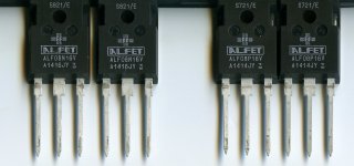
The output fets are ALF08N16V and ALF08P16V lateral MOSFETs from semilab Magnatec. ALFET Lateral MOSFETs.
It looks like the P3 pot is 20R for adjustment JFET source degeneration to adjust H2/H3.
It looks like the P3 pot is 20R for adjustment JFET source degeneration to adjust H2/H3.
Lucky you. Are you clairvoyant? 😀I was by chance a bit prepared…..
The output fets are ALF08N16V and ALF08P16V lateral MOSFETs from semilab Magnatec. ALFET Lateral MOSFETs.
.....
so , basically , any iteration of oldest and bloody popular Hitachi 2SJ50/2SK135 goodies
Lucky you. Are you clairvoyant? 😀
I used the service of a fortune teller from India,
😀😀😀
Lucky you. Are you clairvoyant? 😀
Generg and I are telepathic alien hybrids.
Alfet (ALF series) also made by Semelab.
Last edited:
so , basically , any iteration of oldest and bloody popular Hitachi 2SJ50/2SK135 goodies
Yes, the brand of device is not that important.
There are subtle differences but nothing worth worrying about, use what you already have or have easy access to.
Last edited:
Looks great!! What is the upright component in the middle of the psu pcb, it appears to be in series with one of the AC lines going from switch to the primary of the transformer. Most probably the "noise reducing trick".
It is the thermostat.
😎
- Home
- Amplifiers
- Pass Labs
- First Watt F7 review