Almost back to your first effort in post #136. Do the input jfets gates need a resistor to ground?
Definitely.
Almost back to your first effort in post #136. Do the input jfets gates need a resistor to ground?
No if the signal source is DC coupled to the 100 Ohm gate stopper, yes [e.g. 47K] if capacitor coupled for return to ground. My schematic is an exact copy of lhquam's earlier one in post #136 plus how it works. The lhquam schematic which I hope he did not discard its valuable viability makes full sense; granted it does not oscillate.
The resistor to ground serves two functions:
I am starting to construct a prototype of that circuit using a spare cviller F5c V2.0 PCB for convenience since it uses the DIY UMS board standard and with a few jumpers and minor mods will easily accommodate my F7 experiments.
- Prevents possible problems if nothing is connected to the amp input.
- Helps to define the input impedance of the amplifier.
I am starting to construct a prototype of that circuit using a spare cviller F5c V2.0 PCB for convenience since it uses the DIY UMS board standard and with a few jumpers and minor mods will easily accommodate my F7 experiments.
I have additional explanations [broader pic] on your schematic in post # 136 and/or in # 143 which I'll post tomorrow.The resistor to ground serves two functions:
The schematic of post #143 works quite well, but has a negative input impedance of -10K Ohms. I am currently working on a modification to that circuit that has +10K input impedance and also addresses the -3dB@100kHz issue.
- Prevents possible problems if nothing is connected to the amp input.
- Helps to define the input impedance of the amplifier.
I am starting to construct a prototype of that circuit using a spare cviller F5c V2.0 PCB for convenience since it uses the DIY UMS board standard and with a few jumpers and minor mods will easily accommodate my F7 experiments.
I have additional explanations [broader pic] on your schematic in post # 136 and/or in # 143 which I'll post tomorrow.
The circuit in post #136 cannot work. Both feedback +/- signals are essentially the same and thus the result in partial cancellation with no change to the damping factor. The Rsense resistor introduced in the later circuits is necessary in order to improve the damping factor.
Hint: If you carefully think about the 20W into 8 Ohms specification (rather than 25W for the F5) and the "smooth clipping at 40W/4Ohms" plot in F7.pdf you will realize there is something going on in the output stage to lower the maximum output. Perhaps the Rsense resistor.

Here is a summary of the circuit topologies that I have found to meet the F7.pdf specifications when given the proper components.
The 3 circuits show explicit pathways for positive and negative feedback. Please confirm that the net contribution to output power from both pathways decreases the net power output [20 W/8 Ohm] versus 25 W/8 Ohm for diyF5; as a signature per your hint in an earlier post.
The 3 circuits show explicit pathways for positive and negative feedback. Please confirm that the net contribution to output power from both pathways decreases the net power output [20 W/8 Ohm] versus 25 W/8 Ohm for diyF5; as a signature per your hint in an earlier post.
All three topologies appear to be capable of meeting F7.pdf specifications, including the distortion, output power, soft clipping waveforms, closed-loop gain, damping factor, and -3dB rolloff frequency. Of course, each circuit required as different set of resistor values.
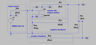
Here is an easy way to simulate the correct value of the positive feedback resistor Rzp. Schematic in post #218 was transfered into a generalized form, given in Mitkopplung20151230g0.png, which is largely expanded in the asc file, see below.
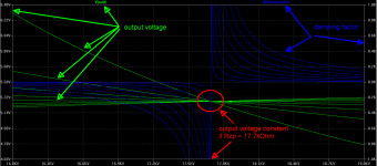
In Mitkopplung20151230g.png a simulation result is shown.
While most of the values of the resistors are given by practical reasons, especially the influence of Rzp and the load RzL are critical on the damping factor and the output voltage. Thus and to keep simulation effort low, different combinations of the 2 resistors shall be simulated in one go. But in LTSpice simulation command DC sweep only active sources can be specified and not resistors. To solve that problem the load resistor and the positive feedback resistor Rzp are replaced in the simulation each by a controllable current source. (Idea: At a given voltage a resistor determins the current according to Ohms law. So a resitor can be replaced by a current source which current is determined by the voltage dived by the resistance, which value is specified by an active source.)
Please notice that as a result the value of Rzp is given on the horizontal axis as kilovolts but is of course in kOhm.
The zip file contains the asc file with explanation and 2 plot files.
To zoom out the simulation result, the command
.dc VTunableResistor1 16000 19000 1 VTunableResistor2 1 8 1
needs to be changed for example into
.dc VTunableResistor1 10 100k 10 VTunableResistor2 1 8 1
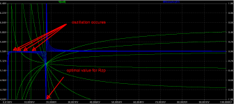
Mitkopplung20151230g1.png shows the result.
In Mitkopplung20151230g.png a simulation result is shown.
While most of the values of the resistors are given by practical reasons, especially the influence of Rzp and the load RzL are critical on the damping factor and the output voltage. Thus and to keep simulation effort low, different combinations of the 2 resistors shall be simulated in one go. But in LTSpice simulation command DC sweep only active sources can be specified and not resistors. To solve that problem the load resistor and the positive feedback resistor Rzp are replaced in the simulation each by a controllable current source. (Idea: At a given voltage a resistor determins the current according to Ohms law. So a resitor can be replaced by a current source which current is determined by the voltage dived by the resistance, which value is specified by an active source.)
Please notice that as a result the value of Rzp is given on the horizontal axis as kilovolts but is of course in kOhm.
The zip file contains the asc file with explanation and 2 plot files.
To zoom out the simulation result, the command
.dc VTunableResistor1 16000 19000 1 VTunableResistor2 1 8 1
needs to be changed for example into
.dc VTunableResistor1 10 100k 10 VTunableResistor2 1 8 1
Mitkopplung20151230g1.png shows the result.
Attachments
Here's a not so easy way to see what's really going on -🙂
Dawid got his paws and camera on it first so voilà:
http://www.6moons.com/audioreviews2/firstwatt2/8.png
Dawid got his paws and camera on it first so voilà:
http://www.6moons.com/audioreviews2/firstwatt2/8.png
The insert at bottom right is the F5 of course.
The bigger one is the F7. Too many parts? But it *works*. Whaddya want?
The bigger one is the F7. Too many parts? But it *works*. Whaddya want?
Looks great!! What is the upright component in the middle of the psu pcb, it appears to be in series with one of the AC lines going from switch to the primary of the transformer. Most probably the "noise reducing trick".
Last edited:

btw
look here , in Bible , entire Chapter 7 :
Radiotron Designer Handbook 4-th edition | Zen Mod Blog
look here , in Bible , entire Chapter 7 :
Radiotron Designer Handbook 4-th edition | Zen Mod Blog
Looks great!! What is the upright component in the middle of the psu pcb, it appears to be in series with one of the AC lines going from switch to the primary of the transformer. Most probably the "noise reducing trick".
temperature switch , what else - already known in other FW amps
besides that ..... 8 resistors , 3 trimpots , plus one resistor for LED - not bad for one channel
CRCC supply , separate banks per channel , Old Bull in action again
- Home
- Amplifiers
- Pass Labs
- First Watt F7 review