Yes I agree with that, but my intention is not to clone F7, but rather build something to my own requirements.
I'll just keep it to myself since the circuit is so bloody simple it won't take much to tweak it in the direction of F7.
In diyF5, negative feedback [NFB] is applied on the joint sources of the input JFETs and not on their joint gates. Same NFB with type 2.This was a good starting point to play with the simulation.
The main difference that I see, from my limited knowledge, between the F5 and the Type 2 is the point where the negative feedback is applied. In the F5 the negative feedback is applied directly on the gates of the jet, while in the type 2 is applied in the center node, that has to be floated with the Rnfbs.
D.
My mistake, I mean source, not gates. But in the diyF5 the nfb is applied just on the source pin of two jfets, while the center is grounded. In the type 2 it goes between the resistors and connected to ground through the rfbs.
Not sure if this is a huge difference.
D
Not sure if this is a huge difference.
D
In my Spice simulations doing F5 there was a bit less distortion with the separate paths of feedback compared to the one way back ticket.....🙂
I never tried to hear this......🙂
I never tried to hear this......🙂
I have a pair of Druids here, recently arrived. Previously having heard
other Zu models, I did not experience how spectacular the Druids are if
you appreciate really articulate midrange without annoying artifacts.
It does take a little work to get the bass right.
These were a pair that had suffered some cosmetic damage to the enclosure,
but Sean will not be getting them back.
😎
I'm working with sean now on a set of fronts that will be paired and powered by the f7. I'm thinking druids or might get crazy with the definitions for the built in submissions.
think it'll be able to get to concert levels in a mid sized room with seans highly efficient speakers? (when i want to)
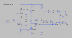
Dear All,
I am trying to simulate the Type 2 feedback scheme applied to a DIYF5. Please note that the value in the pictures are of the F5 adapted to the different mosfet.
I must be doing something wrong, as I would expect the overall gain to increase when I decrease the positive feedback resistor and I get exactly the same behavior.
I am using a dummy speaker load found on stereophile for the speaker.
Thanks,
Davide
Attachments
Dear All,
I am trying to simulate the Type 2 feedback scheme applied to a DIYF5. Please note that the value in the pictures are of the F5 adapted to the different mosfet.
I must be doing something wrong, as I would expect the overall gain to increase when I decrease the positive feedback resistor and I get exactly the same behavior.
I am using a dummy speaker load found on stereophile for the speaker.
Thanks,
Davide
It might seem counter intuitive, but the closed-loop gain decreases as the positive feedback resistor is decreased. To understand this you must consider the voltage produced on the JFET gates from V(In) and V(Out-) through the resistor network. If the target closed-loop gain of the amplifier is 5X (F7 spec) and Rsense=0R3, then V(Out-) = 5*V(In)*.3/(8+.3) = .18*V(In). Now compute V(gates) resulting from the resistor divider (10K and Rfbp) between V(In) and V(Out-).
I see...
I get the following:
Vg= {[ R1/(R1-Rfbp)]*[ (CLG*Rsen)/(Rload+Rsen) - (Rfbp/R1) ]}
Basically Vg (as you said) increase when Rfbp decrease and go to infinite when R1=Rfbp.
So Rfbp=47k will give me 1.22 for 8 ohm load.
Then the game is to solve all the problem to get at a point where CLG and gm are not dependent on Rload any more (If I got all the story right)
Thanks, It's very instructive...
D.
Backwards. I get:
Vgate = Vin * (CLG*Rsen/Rload*R1/Rfbp +1) / (R1/Rfbp +1)
Let A=Rfbp/R1, B=Rsen/Rload then we get
Vgate = Vin*(CLG*B/A+1)/(1/A+1)
= Vin*( A/(1+A)*(1-B*CLG) + B*CLG )
The term 1-B*CLG is positive for all cases of interest, and A/(1+A) is an increasing function for A>0.
Thus, Vgate increases as A increases, and A = Rfbp/R1.
The piece that I am missing in the puzzle is how I calculate gm, that I expect to be also a function of the feedback arrangement and Rload.
Thanks,
D.
Thanks,
D.
Estimating gm is indeed a juzzle since it depends on many variables, the most important being:The piece that I am missing in the puzzle is how I calculate gm, that I expect to be also a function of the feedback arrangement and Rload.
Thanks,
D.
- JFET drain load resistance
- JFET source degeneration
- JFET gm
- Output MOSFET gm
Is there a way to have LTSpice compute gm ?
I understand that it is imperative to remove Rload from the equation, mostly because the real load is frequency dependent.
D.
I understand that it is imperative to remove Rload from the equation, mostly because the real load is frequency dependent.
D.
Backwards. I get:
Vgate = Vin * (CLG*Rsen/Rload*R1/Rfbp +1) / (R1/Rfbp +1)
Let A=Rfbp/R1, B=Rsen/Rload then we get
Vgate = Vin*(CLG*B/A+1)/(1/A+1)
= Vin*( A/(1+A)*(1-B*CLG) + B*CLG )
The term 1-B*CLG is positive for all cases of interest, and A/(1+A) is an increasing function for A>0.
Thus, Vgate increases as A increases, and A = Rfbp/R1.
I am still puzzled by your calculations: let's say that Vgate = F(Rfbp) * Vin
For positive feedback shouldn't I have F(Rfbp) > 1 ?
Thanks,
Davide
I am still puzzled by your calculations: let's say that Vgate = F(Rfbp) * Vin
For positive feedback shouldn't I have F(Rfbp) > 1 ?
Thanks,
Davide
The only requirement for positive feedback is that 1/Rfbp>0, i.e. that Rfpb is non-infinite. What you are failing to consider is that the input voltage V(In) is attenuated by the resistor divider formed by R1 and Rfbp, and that the positive feedback signal from the top of Rsen is the highly attenuated signal V(out)*Rsen/Rload.

This would be a simple way to build a F7-"ish" amp.
I guess this is not the way Nelson Pass builds the F7 since he does not write anything about using 4 JFets per channel. It seems like a simple a neat way to implement some positive current feedback in a F5 inspired amp though.
I know he does not use IRFP parts. I just choose them for a quick simulation.
Cheers,
Johannes

View attachment 536892
This should be better.
I forgot about which input was inverting.....
Cheers,
Johannes
I assume the same mosfets, IRFP9240 M2 and IRFP240 for M1. Jfets J74 and K170?
The IRFP240 and IRFP9240 have a to high Vgs which forces the use of to large values on R1 and R2. There is to much gain with those transistors. I could not simulate the amp with JFets, but with a properly bias mosfet input stage the amp had way to much gain. It became very touchy and wanted to broadcast AM radio for any excuse.
I guess Nelson Pass uses the vertical fets partly to lower the value of R1 and R2. They also drift less with temperature which is important if you want to remove the source resitors.
Seems like a reasonable choice. You might need some resistance between the sources on those Jfets to tame the gain down a bit. I don't have any models for for those Jfets in LTSpice, so i could not simulate them in this circuit. I just pulled the values out of my head. Think of that schematic as general example only. It is not optimized in any way.
Cheers,
Johannes
I guess Nelson Pass uses the vertical fets partly to lower the value of R1 and R2. They also drift less with temperature which is important if you want to remove the source resitors.
Jfets J74 and K170?
Seems like a reasonable choice. You might need some resistance between the sources on those Jfets to tame the gain down a bit. I don't have any models for for those Jfets in LTSpice, so i could not simulate them in this circuit. I just pulled the values out of my head. Think of that schematic as general example only. It is not optimized in any way.
Cheers,
Johannes
- Home
- Amplifiers
- Pass Labs
- First Watt F7 review