I removed what was post #350 showing a PCB layout. I am working on a much more interesting PCB layout for experimenting with a variety of circuit topologies that combine negative and positive feedback, including all of those in post #269, and more.
I removed what was post #350 showing a PCB layout. I am working on a much more interesting PCB layout for experimenting with a variety of circuit topologies that combine negative and positive feedback, including all of those in post #269, and more.
Is it understood that the 3 leading candidate diyF7s you wrote about start as 3 independent diyF5s? Perhaps the PCB you are suggesting will allow an A/B subjective comparison between each parent diyF5, and its descendant diyF7 because each pair [of 3] diffesr by one variable only which is introducing positive feedback.
The schematic shows an idealized version of the amplifier of post #136 that combines both negative and positive feedback. I generated and solved an idealized set of equations for the underlying circuit that assume a perfect differential amplifier with a gain of OLG and output impedance of Rint, and that the positive and negative feedbacks present negligible loads to the output.
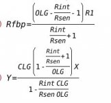
I found a solution for Rfbp (R7) that created an infinite damping factor for the overall amplifier. That is, the output voltage is not affected by the speaker load resistance Rload. The solutions for the positive feedback resistor and the output voltage are interesting in that they only depend on the open-loop gain OLG, CLG, and the ratio Rint/Rsen. CLG is the approximate closed-loop gain given by negative feedback network:
CLG = 1 + Rfbn/Rfbs
I find this to be a very interesting result.
Attachments
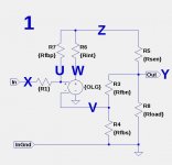
The schematic shows an idealized version of the amplifier of post #136 that combines both negative and positive feedback. I generated and solved an idealized set of equations for the underlying circuit that assume a perfect differential amplifier with a gain of OLG and output impedance of Rint, and that the positive and negative feedbacks present negligible loads to the output.
I found a solution for Rfbp (R7) that created an infinite damping factor for the overall amplifier. That is, the output voltage is not affected by the speaker load resistance Rload. The solutions for the positive feedback resistor and the output voltage are interesting in that they only depend on the open-loop gain OLG, CLG, and the ratio Rint/Rsen. CLG is the approximate closed-loop gain given by negative feedback network:
CLG = 1 + Rfbn/Rfbs
I find this to be a very interesting result.
Thank you lhquam for this excellent and admirable work. Suppose R7 [for +ve feedback] is removed. Then Rint + R5 [sense] may be summed as they are in series to equal a new internal impedance for the amp. The resultant amp is a diyF5 which is the accepted parent or precursor of diyF7. How do the objective data for this diyF5 compare with its resulting diyF7? How many dBs of positive feedback are you allowed before this diyF7 oscillates?
I found an error in circuit model. The differential amp I used was a voltage amplifier Vout(V+,V-) , but it needs to be a transconductance amplifier Iout(V+,V-), corresponding to the behavior of the output MOSFETs. Stay tuned.
Yes there is an equilibrium set of values where the load is cancelled out of
the equation.
I have to admit, however, that I arrived at it through trial and error, one simple
equation for inverting, another for non-inverting. A trimpot takes care of the details...
😎
the equation.
I have to admit, however, that I arrived at it through trial and error, one simple
equation for inverting, another for non-inverting. A trimpot takes care of the details...
😎
Yes there is an equilibrium set of values where the load is cancelled out of
the equation.
I have to admit, however, that I arrived at it through trial and error, one simple
equation for inverting, another for non-inverting. A trimpot takes care of the details...
😎
What is nice is to have an equation to get close to the desired values before tweaking with the trimpot. 🙂
...That's why I hide anything I don't want you to see.
😎
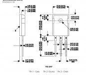
In the F7 4 MOSFETs share 160W, so each has to carry a load of 40W, which is times more than in other amps. Is it that we don't see additional MOSFETs on the underside of the pcb? Or are the ALFETs just tougher?
Ha, ha, you see same laughing like picodumbs......😀
the drain and source of the Alf08N/P16 are changed, look here.....
one fuse killed....
Hu, hu two Alfs also dead....
I burried them at the same place as the fuse.......😡😡
But two pairs are still stored in the basement, so the show goes on.....this afternoon.
😀🙂
Mind the right pin order!
Thanks for the heads up on the ALFET pin order issue. I wonder why they did that.
All lateral mosfets have that arrangement (dumb bastards). hahahaha
Let us assume 1.2A and 48V so we have around 60W for two, means one Alf only 30W.
Because reverse engineering is somewhat funny, I will do a little hair splitting:
F7.pdf says 160W total for the amp. Transformer consumes maybe 10%, leaves 144W for the rest. Rectifiers will use roughly 1V(=Uf)*2A(160W/2 (number of rectifier bridges) /2*Ubatt)*2(numer of diodes per bridge)*2(number of bridges)=8W, leaves 136W for the 4 MOSFETs, i.e. 34W per MOSFET.
34W is a lot for one MOSFET.
You cannot handle 48V with the JFETs. The original F5 had about 35W per output FET. How about 25V rails and 1.4A bias?
All lateral mosfets have that arrangement (dumb bastards). hahahaha
The 6Moons photos leave you scratching you head about the position of the V+ and V- connections relative to the ALFET pins. It sure looks like rail connections to the 3rd pin with is now known to be the drain pin. Of course we do not know what is on the backside of the PCBs.
Because reverse engineering is somewhat funny, I will do a little hair splitting:
F7.pdf says 160W total for the amp. Transformer consumes maybe 10%,
No transformer has efficiency of 94.75%.
If you look up typical efficiency of linear power supplies, the bias figure is closer to 1-1.1A per channel.
That at least would be my guess.
- Home
- Amplifiers
- Pass Labs
- First Watt F7 review