difficult to find complementary mosfet in indonesia pak Thole?me too
I have never tried small IRFs (540/9540, 640/9640) but they are easy to find in Glodok.
Quasi (all N-channel) is not necessary, unless you already have the parts in stock. Toshiba 5200 is cheap, fast (suitable for CFA), original and sounds beautiful.
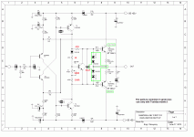
Very nice and reasonable PCB! PWR Ground with high current tracks does not go near (or around) small-current signall paths, as usual seen in other Layouts.
Have you tested it?
If it is working could you share the Egle file or PDF.
p.s. It's good idea to add Gate/Base stoppers and VBE transistor for thermal compensation if used in Class AB operation.
Have you tested it?
If it is working could you share the Egle file or PDF.
p.s. It's good idea to add Gate/Base stoppers and VBE transistor for thermal compensation if used in Class AB operation.
OK, shortened the track lengths for C9/C10 and used SMD bypasses on the underside as suggested - however, size of C9/C10 had to be reduced from 16mm to 12.5mm to get the most placement benefit. That's probably OK, since there's enough choice of 470..1000uF, 50 to 63V caps in 12.5mm.
The overall dimensions are down to 2" x 2" (~50mm x 50 mm), which seems to be close to optimal for the layout, allowing interchangeable use of TO3P and TO247 outputs..
p.s. It's good idea to add Gate/Base stoppers
linuxguru, I wanted to say, that Gate/Base stopper resistors should be as near as possible to base/gate leg of transistor. In You layout these resistors are a little bit away from it.
Yes,my stage is biased in class B,so not current on output transistors.
<..>
I tried to use two diodes.I don't hear any changes in sound.
With 3 diodes I've got 6 mA (through NPN) and 2.5 mA (PNP) transistors.
With 2 diodes I've got 2 mA (NPN) and 0.05 mA (PNP)
So it's like Class AB, no crossover (step) distortion on output even with small (0.01V) input signal.
I have changed Darlington transistors to Mosfets (IRFP) and have got crossover distortion even with 3 diodes and no current at output transistors at all. This is Class B operation 🙂
Ok I have a silencer to change on my car this afternoon and I do the simulation on the other.
Please do not forget to sim my circuit if you have time
Thank you🙂
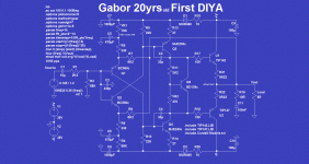
I post the circuit here for now, in case someone has interest there is a thread on the amp.
To me sound fantastic but need some tweak to make it 100% stable..😱 THESE circuit already include some mode to be more thermal stable, that NOT TESTED YET!
Greetings
Attachments
gaborbela
Why You are using so high impedance NFB network resistors ? 15k/330R.
I do not have a time to sim it but it is so simple amplifier that you can just plug it in and measure the currents. The stability should be fine, it is bulletproof design.
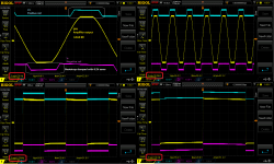
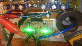
I am working on the high efficent hexfet ops with double bootstrap (for subwofer amplifier), first tests are passed OK. I will have to prepare another board and get a few more of mosfets at the OPS. The output swings nearly from rail to rail (screanshots with single pair of mosfets only). The temperature stability is rock solid!
More reports end of the week.
Why You are using so high impedance NFB network resistors ? 15k/330R.
I do not have a time to sim it but it is so simple amplifier that you can just plug it in and measure the currents. The stability should be fine, it is bulletproof design.
I am working on the high efficent hexfet ops with double bootstrap (for subwofer amplifier), first tests are passed OK. I will have to prepare another board and get a few more of mosfets at the OPS. The output swings nearly from rail to rail (screanshots with single pair of mosfets only). The temperature stability is rock solid!
More reports end of the week.
Attachments
Hi Boris
Here is a modified version which simulate very good to.
I'm not sure if the VBE correct I mean if is good enough to take care of any of previous thermal drifts.
Please take a look.
Of course I appreciate your comment and help!!!🙂
Greetings
Here is a modified version which simulate very good to.
I'm not sure if the VBE correct I mean if is good enough to take care of any of previous thermal drifts.
Please take a look.
Of course I appreciate your comment and help!!!🙂
Greetings
Attachments
If it simulates good just make the board for it, the temperature compensation can be easily matched on the real life amp
post573
R20 is the Hawksford/Hagerman/Self added resistor to compensate the Vbe multiplier for variations in multiplier current.
As such the tappings to feed the next stage are connected to the emitter and collector of Q9.
The sch shows the upper tapping connected to the wrong side of R20.
C17 & R22 should connect to the bottom end of R20.
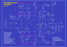
Hi Borys
We need your help with the Hawksford/Hagerman/Self added resistor R20..
How you can see Andrew wrote that is incorrect.
Would you please take a look...........
The first circuit how you implemented originally, the second how I understood Andrew's advise.
Thank you 🙂
Cheers
Attachments
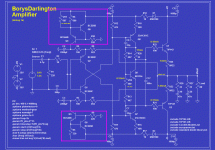
The Andrew is correct. The R20 resistor role is to improve bias thermal stability.
As far I remember I was not using that resistor in this amp (maybe I have short memory).
In my EF3 OPS this resistor was indeed improving the thermal behavior but it was also causing OPS oscillations (in that case it was not a good idea).
Remember that You can also adjust the thermal compensation by changing the R14 and R13 values (they go in parallel with bd139), or plan B is use mje340 instead of bd139 it has lower tempco.
BTW the R14 and R13 network was for the IRF Vbe, here the value of R13 will have to be lowered to get the OP transistors biassed up.
Cheers
Last edited:
can I have the schematic of bootstrapped version which had high distortion you mentioned in post 645
Last edited:
suresh
When I get back home I will post U a new schematic. I must know the operating voltage You are going to use to match the bootstrap resistors.
There is a new simple IPS in progress, very fast VFA!! If you can wait a few days there will be a new version.
The bimo's symetri is well tested also so it can be melted into the one integrated board.
Distortion figures are really decend.
Attachments
suresh
When I get back home I will post U a new schematic. I must know the operating voltage You are going to use to match the bootstrap resistors.
There is a new simple IPS in progress, very fast VFA!! If you can wait a few days there will be a new version.
The bimo's symetri is well tested also so it can be melted into the one integrated board.
Distortion figures are really decend.
Hardly wait on that! 🙂
Thanks Peter
Darlington Output & Thermal Drift
If I remember well, Classe DR3 with Darlington Output stage had a Vas Multiplier and temperature sensing with a darlington transistor MPS serie and the DR£ Very High Current version had only a resistor as thermal sensor and no Vas Multiplier. I see no reason for a well designed amplifier to drift other than normal level. I'm wrong?Please do not forget to sim my circuit if you have time
Thank you🙂
I post the circuit here for now, in case someone has interest there is a thread on the amp.
To me sound fantastic but need some tweak to make it 100% stable..😱 THESE circuit already include some mode to be more thermal stable, that NOT TESTED YET!
Greetings

Great work, platon.rado!
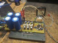
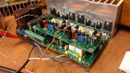
p.s. Only onboard PCB Big electrolytic capacitors are looking "too big" 🙂
p.s. Only onboard PCB Big electrolytic capacitors are looking "too big" 🙂
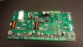
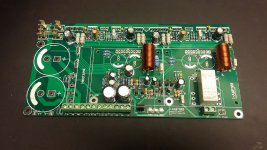
Now the new version is comming --> iAMP100. The stereo OPS unit for single pair transitors, just transformer is required.
The board will ''take'' on board BJT and the Mosfet transitors, board has:
-main PSU
-preamp PSU +/-15V with short circuit protection
-speaker DC protect
-over temperature protect
-speakers 10s delay ON
-speakers fast OFF -->after trafo is switched OFF
-you can use single relay or two separete relays
-BJT or FET-hex output transistors
IPS boards are 60mm x 70mm which is enough to fit in most of the simple amplifiers (including sony ta777es if you will have a parts 😀 ).
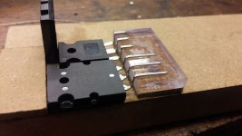
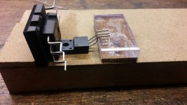
The special tool will help to bend the transitor legs 😀 (spacers distance is 30mm)
The board will ''take'' on board BJT and the Mosfet transitors, board has:
-main PSU
-preamp PSU +/-15V with short circuit protection
-speaker DC protect
-over temperature protect
-speakers 10s delay ON
-speakers fast OFF -->after trafo is switched OFF
-you can use single relay or two separete relays
-BJT or FET-hex output transistors
IPS boards are 60mm x 70mm which is enough to fit in most of the simple amplifiers (including sony ta777es if you will have a parts 😀 ).
The special tool will help to bend the transitor legs 😀 (spacers distance is 30mm)
Attachments


Last edited:
- Home
- Amplifiers
- Solid State
- FET-hex explendit amplifier