Sorry[/QUOTE
Hi Borys ,
Sorry,
What is the programme to open these files? I download and unzip these file but cannot read them .
thanks
kp93300
PCB-copper to be in pdf
Hello mr Borys!
Hole to be the drill 1mm.
Please PCB-botton (copper) to be in pdf
thank you and cheers!
Hello mr Borys!
Hole to be the drill 1mm.
Please PCB-botton (copper) to be in pdf
thank you and cheers!
Last edited:
fet hexfet
You need, CadSoft EAGLE PCB Design Software.Sorry[/QUOTE
Hi Borys ,
Sorry,
What is the programme to open these files? I download and unzip these file but cannot read them .
thanks
kp93300
www.cadsoftusa.com
Or borys can export PDF from this.
Last edited:
PDF f's
Just do not forget to put zobel network 10R+100nF and coil at the output (16-19 windings on 5mm diameter resistor 10R).
You can putt that on the amp terminals or on psu board (my case is on psu).
Both pcbs you can use for mosfets (toshiba in my case) but only one for BJT.
I think BJT board is better but bit bigger.
Attachments
-
bottom.pdf62.3 KB · Views: 370
-
BG1-bjt top.pdf47.7 KB · Views: 370
-
BG1-bjt schematic.pdf12 KB · Views: 518
-
BG1-mosfet top.pdf44.2 KB · Views: 346
-
BG1-mosfet schematic.pdf11.8 KB · Views: 518
-
bottom BG1 bjt.pdf70.2 KB · Views: 357
-
 bg1 bjt mos with drivers.jpg217.2 KB · Views: 1,368
 -
 bg1 mos.jpg130.4 KB · Views: 1,308
 -
 bg1 taz.jpg128.4 KB · Views: 1,266
Last edited:
Last edited:
I tested my another amp today,and it's necessary to add 330pF on C and B of outputs.If no this,amp will oscillate and destroy.My first amp not needed this cap because transistors have low fT.
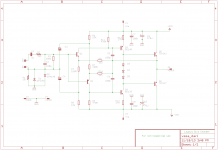
Acca, thanks for your Darlington schematic. I used a discrete Self Type-II Darlington biased to Class-B in my LTSpice simulation schematic (.asc attached below), and I can confirm that it is now stable. The only change I made to obtain unconditional stability is Cherry-type compensation C4, C5 directly from outputs to the bases of the VAS transistors. Any value from 10s to 100s of pF will work - this allows fast BJTs to be used, and the compensation also has the bonus effect of reducing Class-B crossover distortion. Without C4 & C5, the phase response shows a small kink in the MHz region, which is probably what causes the instability with fast BJTs.
(Of course, the physical build can use integrated fast Darlingtons like Sankens, instead of the discrete Darlington shown in the simulation schematic - I don't have Spice models for the Sanken Darlingtons, which is why I used the discrete Darlington shown for simulation.)
Attachments
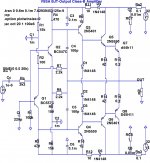
I was also thinking this days to Acca's diagram using some STD03N/P that I have around. They have integrated bias diodes, and E terminals close to each other.
Thanks for the compensation tip, linuxguru
Thanks for the compensation tip, linuxguru
Thanks for the compensation tip, linuxguru
You're welcome.
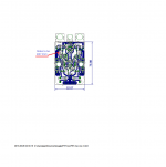
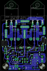
Here's a first-pass layout of a Darlington VSSA (some things still have to be refined, including additional device flexibility for the Darlingtons and some of the caps, but placement looks OK and the size is compact at 2.4" x 2.4" (~60mm x 60mm). It's completely single-sided with no via or jumper.
If there's any error, omission or something that would be nice to include/change on this layout, please post it here over the next 2-3 weeks, and I'll try to incorporate the change before sending it off for fabrication in December.
Attachments

You're welcome.
Here's a first-pass layout of a Darlington VSSA (some things still have to be refined, including additional device flexibility for the Darlingtons and some of the caps, but placement looks OK and the size is compact at 2.4" x 2.4" (~60mm x 60mm). It's completely single-sided with no via or jumper.
If there's any error, omission or something that would be nice to include/change on this layout, please post it here over the next 2-3 weeks, and I'll try to incorporate the change before sending it off for fabrication in December.
Nice layout of pcb tracks.
Where do you put the heatsinks for the VAS transistors?
It would be good to have the option for a bce to-220 device for VAS...
Why so high value for R3, R12 and R13?
If we want to use vertical Fets instead of darlington BJT it would be good to have an option for VBE multiplier with R in series... The fet would be 2sk1530/J201.
Thanks
Fab
Last edited:
Where do you put the heatsinks for the VAS transistors?
It would be good to have the option for a bce to-220 device for VAS...
Why so high value for R3, R12 and R13?
If we want to use vertical Fets instead of darlington BJT it would be good to have an option for VBE multiplier with R in series... The fet would be 2sk1530/J201.
I'll leave space for a small bolt-on heatsink for the TO126 or TO220 VAS transistors - Iq is less than 10 mA through these, AFAIK. Even at 45V, that's less than 0.5W Pd.
IIRC, Lead spacing is the same for both TO126 and TO220 (?), so TO220 devices can interchange with the BD139/140 TO126 BCE pinout devices, and I'll adjust clearances to allow that.
Component values can be anything the builder chooses - However, R3 was kept at 100k to limit attenuation from the 3k3 input resistor. All those values are at the builder's discretion.
Vbe multiplier - would you recommend a stock NPN + 2R mulitplier, or maybe just a resistor in series with the diode chain?
FETs - would they need gate stoppers and/or zener protection for the gates?
To-220 and to-126 have a different pin out ( bce vs ecb) so it makes a difference when put on an heatsink. 10ma may be ok for Vas for darlington BJT but for a MOSFET with no driver I prefer the current in the range of 25ma.
100k for input may be not enough for optimized bias for input BJT.
I prefer the transistor to-126 BJT NPN for multiplier since it can be in contact with main heatsink for temperature compensation. The R in series with the transistor is for the output FETs to prevent over-compensating.
Yes it would need gate stoppers and even base stoppers...
The Zener are a good idea in case they are not already included in the MOSFET.
Fab
OK, added base/gate stoppers for the output devices. Also managed to squeeze in gate-protection zeners. The overall board size has been crunched a little to 2" x 2.4" (~50mm x 60mm), and I'll stop there - I already had to reduce the lengths of a bunch of resistors to 7 mm.
Vbe multiplier is still hanging in the air - for anything other than Class-B, it will need thermal compensation and have to be mounted between the power devices on the heatsink, which messes up the existing track routing. For Class-B, the 3- or 2-diode chain is adequate for darlingtons/lateral FETs, and a zener is adequate for vertical/DMOS FETs - all of these can be mounted easily in the existing 3-diode chain. So I'll defer the Vbe multiplier, but have retained some space to include it as a future plan B.
VAS heatsinks should be OK for TO126, and there are already good medium-power transistor choices in TO126 including BD139, 2sb669, 2sc2690, etc.
Some more cleanup has to be done, including pad diameters, track widths, clearances, text, and component length flexibility for the input coupling cap C1, but placement looks better and routing is also moderately tight - it should be good to go within a week.
Edit: Just noticed that 2sk1058/2sj162 have GSD pinout (instead of GDS used on say the IRFP240/IRFP9140, which allows them to be directly substituted for darlingtons with BCE pinout). So that rules out the Hitachis, unless an additional set of jumpers or pads is provided to interchange D & S pins. That would be messy and increase the board length.
Attachments
Last edited:
So that rules out the Hitachis ...
However, 2sk1530/2sj201 Toshiba verticals have GDS pinout with 5.45mm spacing, so they should be good to go as drop-in replacement for the darlingtons, with suitable changes to the gate-stopper resistors, gate-to-gate bias-voltage chain and the VAS quiescent current.
(This must be old hat to most people here, but I've never used laterals, so the pinout difference came as a bit of a surprise to me).
OK, added base/gate stoppers for the output devices. Also managed to squeeze in gate-protection zeners. The overall board size has been crunched a little to 2" x 2.4" (~50mm x 60mm), and I'll stop there.....
Edit: Just noticed that 2sk1058/2sj162 have GSD pinout (instead of GDS used on say the IRFP240/IRFP9140, which allows them to be directly substituted for darlingtons with BCE pinout). So that rules out the Hitachis, unless an additional set of jumpers or pads is provided to interchange D & S pins. That would be messy and increase the board length.
Hello linuxguru,
Nice layout You made, maybe a good idea would be to place a zeners directly on the OPS TRs pins on top or bottom of the PCB (pads located on OP TR pads with a little offset to the OP TR pin holes, the C7 and C8 should be mounted on the bottom of the board directly to the main C9 - C10 (SMD would be even better) Caps same little offset for the pads holes to be near Bigger Elcos holes. This way You can move the main C9 - C10 Caps almost on top of the OP TRs minimizing the pulse ringing while loading the caps - and gain some additional space or shorten the power tracks or PCB accordingly and still preserve Single side PCB. AS this is wide band design each mm shorten of the track length matters much.
With my best regards,
A.
... You can move the main C9 - C10 Caps almost on top of the OP TRs minimizing the pulse ringing while loading the caps - and gain some additional space or shorten the power tracks or PCB accordingly and still preserve Single side PCB. AS this is wide band design each mm shorten of the track length matters much.
OK, shortened the track lengths for C9/C10 and used SMD bypasses on the underside as suggested - however, size of C9/C10 had to be reduced from 16mm to 12.5mm to get the most placement benefit. That's probably OK, since there's enough choice of 470..1000uF, 50 to 63V caps in 12.5mm.
The overall dimensions are down to 2" x 2" (~50mm x 50 mm), which seems to be close to optimal for the layout, allowing interchangeable use of TO3P and TO247 outputs..
Attachments
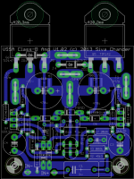

The overall dimensions are down to 2" x 2" (~50mm x 50 mm), which seems to be close to optimal for the layout, allowing interchangeable use of TO3P and TO247 outputs..
Excellent,
Very compact and elegant design 🙂
Now only the preliminary real life test and for sure many Diyers will be satisfied with Yours elegant and compact PCB Artwork,
Congratulations,

With my best regards,
A.
@ borys
Thank you for the good job done for us in the forum.


On Nov. 03rd you postet the PDF-files of the amp, but by accident there is the wrong PDF-file of the BJT-amp-version. Please post this file to us Thanks.

Thank you for the good job done for us in the forum.
On Nov. 03rd you postet the PDF-files of the amp, but by accident there is the wrong PDF-file of the BJT-amp-version. Please post this file to us Thanks.
BJT version bellow. In case You will have problem to get correct bias replace R19
with 100-220R. In case of mounting VAS transistors above pcb you can put 22R resistors intstead R4 and R5. For vas and drivers get transistors with as high gain as possible (around 200 will be perfect). Compensation caps can be 22-33pF. And do not forget to put zobel network + coil at the amp terminals.
I think next very easy step to improve the amp would be to cascode the vas to separate it better form input stage (just 2 transistors, 2 diodes and one resistor)
Regards
Attachments
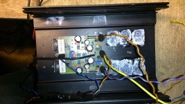
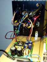
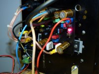
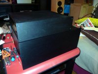
Hi all, it pass a bunch of time that parts are soldered on Versatil PCB (=BG1-MJL with new gnd layout for first stage and same caps profil as LC-VSSA (nichicon and 10uF MKT)).
Recently i bought 2u SMPS300RE and this week i decided to put all together. That i do and all i can say is that combo is amazing, really outstanding combo. It outpass all what i done up today....
Yet it's time to install it in decent housing...i bought some Hifi2000as i lake of time to custom one and i hat to see all these wire in air...
Marc
Attachments
- Home
- Amplifiers
- Solid State
- FET-hex explendit amplifier