
Dead Channel on new build.
Before I start a deconstruction process, I would like to try and narrow down the reason why my Board A is not producing sound. So far I cannot find an answer in this thread.
I went through and checked the voltage across all of the component except for caps, transformers and transistors Q3/Q4. Cap are in the correct polarity. I could not find any differences measuring DC voltage.
I do need to organize the wiring after solving this issue.
Any suggestions on next steps? The working channel sounds great.
Thanks,
Jeffri
Before I start a deconstruction process, I would like to try and narrow down the reason why my Board A is not producing sound. So far I cannot find an answer in this thread.
- I spent the last two days dialing in the bias and offset with no issues.
- Power source is working as it should, +/-24V, all the lights light up, Biases at 0.600V, Offset ~0mV, temperature on heatsinks ~49 degree C
- As a preface, I have swapped/switched speaker and input cables, speakers, and preamps.
- I have checked the continuity of the RCA inputs to the boards and speaker outputs.
- I used the kit from used DiyAudio Store, V2 board.
I went through and checked the voltage across all of the component except for caps, transformers and transistors Q3/Q4. Cap are in the correct polarity. I could not find any differences measuring DC voltage.
|
Any suggestions on next steps? The working channel sounds great.
Thanks,
Jeffri
Attachments
-
 IMG_20240127_140807071_HDR.jpg529.5 KB · Views: 130
 -
 IMG_20240127_140931690_HDR.jpg631.9 KB · Views: 132
 -
 IMG_20240127_140757988_HDR.jpg487.1 KB · Views: 129
 -
 IMG_20240127_140912321_HDR.jpg501.4 KB · Views: 115
 -
 IMG_20240127_140842425_HDR.jpg502.7 KB · Views: 113
 -
 IMG_20240127_140821478_HDR.jpg533.4 KB · Views: 128
Have you checked the resistance of the 4 windings on the Jensen transformer - they should all measure around 28 to 30 ohms on each winding.
No I have not. Can you explain the procedure to do this? There are 4 visible "pins" extending from each side of the transformer. Does one measure resistance across to the corresponding pin? Or measured on the soldered points? Is this done with out the amp turned on?
Thanks.
Thanks.
Measure the resistance with a DMM with no power on.
Pin 1 of the transformer is the one with the smaller distance to its adjacent pin 2 - so one side has pins 1 to 4 and the other side has pins 5 to 8 (pin 5 is opposite pin 4)
Now measure resistance of pin 1 to pin 3. Then pin 2 to pin 4 - on the other side pin 5 to pin 7 and finally pin 6 to pin 8.
As I said each of the 4 measurements should reveal a resistance of 28 to 30 ohms, but once the transformer is in circuit that might change with parallel resistor paths. You are looking for a resistance on all 4 windings and no open circuits.
I would measure at the pcb solder joints, as this will measure the winding and its solder point at the pins on the transformer.
If these all measure OK, then I would carefully recheck , reflow all solder connections seeing you show consistent voltage readind for each channel.

Ok I couldn't wait. At the PCB joints, the resistances between pins 1-3 and 2-4 are 12.4 ohms. Between pins 5-7 and 6-8 the resistance is 29 ohms.
Last edited:
two primaries are in parallel so, 29//29, goes pretty much close to your 12R9, considering there are some other things left is surrounding circuit
secondaries are also OK
arrange some sort of signal generator for anything in between 300Hz to 1KHz (PC file, CD), so you can measure with DVM set to Vac
inject said signal in powered channel, say 100-200mV
no load on output
measure signal at input pads of channel
measure signal at buffer output, ref. to GND
measure signal across primary
measure signal across each secondary
inform here
Last edited:
Nothing wrong with the transformer - that is good news.
ZM is asking you to inject an AC signal at the input and measure with a DVM set to ACV at the 4 points in the circuit he has listed, with no load connected to the output.
This will lead to where the signal is being lost on the faulty channel.
I just measured an F6 pcb here with the Jensen and my results are:
Primary
pin 1 to 3 = 14.5R
pin 2 to 4 = 14.5R
Secondary
pin 5 to 7 = 29.5R
pin 6 to 8 = 29.3R
Your 2 primary windings in parallel seem low at 12.4 R. Looking at the circuit the only thing that can affect the primary winding resistance where they are in parallel is the 2 JFets - are these inserted in the correct P/N position and not in backwards. You would expect the 2 primaries in parallel to read half the winding resistance - which is what they do on my finished F6 pcb here.
Last edited:
You are getting 300mV at the input to the Jfets it seems but nothing out of them as the primary has measured 0mV and therefore 0mV on the secondary windings.
I suspect the Jfets - are they legitimate Toshiba or LS Jfets?
Something is amiss around the input Jfets on that channel.
Reflow the solder again, make sure Q3 is the 2SK and Q4 is the 2SJ.
Compare signals on the good channel to the faulty one - that might lead you to the problem.
Do you have new Jfets to try as a last resort?
Zen Mod might have more to add.
Cheers,
Gary.
Gary, Thanks for your replies (even to the one I removed).
I am awaiting new JFets. I tried to determine if the JFETS were indeed the issue, however I have burned up three R4 resistors, the 18R 1/8W (I put some 1/4W in and they cooked also). Does this indicate something related to the JFETS? Time to check the board again for a short?
I am awaiting new JFets. I tried to determine if the JFETS were indeed the issue, however I have burned up three R4 resistors, the 18R 1/8W (I put some 1/4W in and they cooked also). Does this indicate something related to the JFETS? Time to check the board again for a short?
Looking at the schematic in post #1, if either input JFet was short then you would get a current path from the rail voltage through the parallel primary windings on the Jensen transformer then through R4 (18R) to GND - that would produce a current of around 0.7 amps dissipating around 12 watts in the windings and 12 watts in R14. So I would definitely install new Jfets and also check the windings resistance again.
Just got my calculator out - so if a Jfet was short, you would have the 2 primary windings in parallel = 14.5R ( 2 x 29R in //) in series with R4 (18R) to GND. With a 24VDC supply rail, that is a combined resistance of 32.5R. At 24VDC the current would be 0.74Adc (E/R) This will give a voltage across the parallel windings of 10.73Vdc and 13.32 Vdc across R4. Ohms law then will give you a power dissipation (ExI) in the windings of 7.95watts (3.975w per winding) and 9.86 watts in R4. I got the diss wrong above when doing sums in my head quickly.
If this was sustained, the windings most likely will be damaged, but fortunately R4 being 0.25W will pop very quickly with a dissipation of 9.86 watts and this will be acting as a fuse - and the windings should be OK, but double check them again.
It is likely only one of the 2 jfets has caused this, because if both were shorted, then you would have a direct short across the +/- 24VDC rails. I assume your PSU is +/- 24VDC.
Thanks for the calculations and explanation. This makes great sense, and I have ordered new JFETS and will replace the lot. Hopefully no other damaged components.
Good luck with the repairs, and while you are at it, double check the faulty channel pcb for good solder joints, and no other shorts.
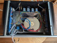
Hi All, the earlier problems are fixed replaced the MOSFETs and the heat pads.There is definitely something off with Q1. Do you have another mosfet for replacement?
Remove Q1 and before replacing it, power up and check the voltage across the zener, Z1. If it is a 5.1V zener, it should measure 5.1V +/- 5%.
By the way, when you measured the mosfet Vgs, if you had the black probe on the gate and red probe on the source, the measured voltage should be negative.
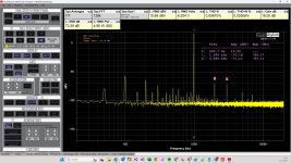
Did some measurements and they come close with other F6 measurements.
Only the 50hz and 100hz peak are high. Any tips on that?
Maybe shorter transformer cables?
Transformer vertical?
Attachments

It's great that it is up and running.
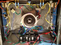
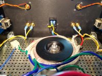
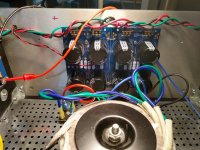
It looks like the 100Hz is much higher than the 50Hz noise, and there appears to be many harmonics of the 100Hz. Your power transformer is enclosed, so that is good. I suggest rotating the power transformer 90 degrees counterclockwise so that the transformer secondary wires are exiting toward the front of the amplifier. Also move the PS output wires to amplifier boards and speaker out wires away from the power transformer and rectifiers.
I see what appears to be the PS board ground wire to chassis ground, but the connections to the PS board and chassis are not visible. A picture of the PS board and the chassis ground point would be helpful.
- Home
- Amplifiers
- Pass Labs
- F6 Illustrated Build Guide