Thank!
Two more questions:
1) with 18V on secondary and CRC filtering with 0R125 can I use 4x 22kuf@35V before R and 4x 33kuf@25V after? Or it is safer to use 8x22kuf@35V?
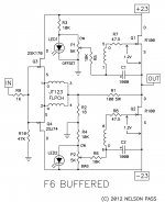
2) Are these blue LEDs good for F6 TLHB4201 Vishay Semiconductors | Mouser ?
Two more questions:
1) with 18V on secondary and CRC filtering with 0R125 can I use 4x 22kuf@35V before R and 4x 33kuf@25V after? Or it is safer to use 8x22kuf@35V?
2) Are these blue LEDs good for F6 TLHB4201 Vishay Semiconductors | Mouser ?
@buzzforb
Regarding your exercise in frivolity 😀😀 - are you saying lift the ground at the junction of R2 and R4 and connect to the mirrored side( same point)?
To me one of the incentives to do a BBA3 was that supplied with a SE signal the circuit would act as a unbalanced to balanced converter. Will the "balanced F6" act in the same way.
Hope I am not way off base
Thanks
Bob
Attachments
You are correct.
Question of performance for m was around how the xformer would handle error current. Mr T kindly sent me two F6 boards loaded ervything but the outputs. I wil be using laterals to test the idea. Will make a little jumper to ty the two boards together.
Yes, you can drive it with SE.
It rally is more about a concept than anything. I also considered that the extra gain from the two sides would allow for low gain fets like laterals and Cree Sic devices, but i could be off base in my thinking.
I have some old school Vfets I need to get creative with. I mean i got to go copy something😀
Last edited:
Thank!
Two more questions:
1) with 18V on secondary and CRC filtering with 0R125 can I use 4x 22kuf@35V before R and 4x 33kuf@25V after? Or it is safer to use 8x22kuf@35V?
2) Are these blue LEDs good for F6 TLHB4201 Vishay Semiconductors | Mouser ?
I dont see any advantage in mixing values. Cost is not good reason. 18V will give almost 24V rails, so i tihnk the 35V caps are better idea.
Red or green is preferred color for noise. If you dont have SS Jfets, then blue is what is need, i believe. You could always just use a zener. Just different type of votlage reference.
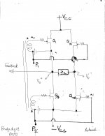
Bridge DIY F6
Does one need two diy F6 amplifiers to make a bridge amp? The attached diagram shows that one assembled diy F6 plus two loose R100A may only be required. Please consult the diagram, and note the following:
Best regards
No worries, either will work. Just a diode.
@Antionel
Thats from the world of buildit😀
Does one need two diy F6 amplifiers to make a bridge amp? The attached diagram shows that one assembled diy F6 plus two loose R100A may only be required. Please consult the diagram, and note the following:
- Q1, Q2 and the transformer are part of an assembled diy F6 as we know it.
- Q1A and Q2A are the two additional R100A needed to make the bridge amp.
- Point P1 [upper FET in F6] provides Q1A with bias, a signal which is out of phase with that on Q1's gate, and is within the feedback loop of diy F6.
- Point P2 [lower FET in F6] has the same attributes of P1 above.
Best regards
Attachments
There is another reason for connecting them this way. I like your idea, even if I am unsure it will work. Thats not to say it won't, just unsure. What happens to V gain.
Thanks buzzforb. Good question about V gain. Maybe the circuit can be initially SIM'ed to unravel its potential.There is another reason for connecting them this way. I like your idea, even if I am unsure it will work. Thats not to say it won't, just unsure. What happens to V gain.
You just lost me🙂
- Can the bias circuit for the bottom FET Q2 [diy F6] simultaneously bias Q2A [as in my drawing above]. Most probably yes; because this lower bias circuit is referenced to -Vcc.
- Can the secondary transformer winding for the bottom FET simultaneously present an out phase signal to the gate of Q2A [as in drawing]. Most probably yes.
- So when Q2 is progressively turned on, Q2A is simultaneously and progressively turned off. And the reverse with signal phase reversal.
- Bias Q1A using its independent circuit exactly like that used for Q1.
- Borrow a winding from the Front End circuit. Connect it to Q1A exactly like that for Q1; except reverse its phase to that presented to the gate of Q1
- Now Q1A and Q2A are most probably biased and signal phased for proper operation
I meant about the SIM.😉 Lets say that all the above is true. What difference do you expect in performance. What does this bring to the table to warrant the change?
buzzforb; I do not know yet the answers to your relevant questions; but I will think about them. To start, I saved a Jensen and a bias circuit, and thus simplified the circuit; but what else gives in return?. It is easy for me to scribble a schematic, fumble and redo until it sits right. It is just a suggested bridge diy F6.I meant about the SIM.😉 Lets say that all the above is true. What difference do you expect in performance. What does this bring to the table to warrant the change?
I am not trying to be crtical. My rip off circuit may be a waste as well, but i do know it has a few possible advantages. Balanced input, distortion reduction. THe main concern is that you may lose some of the harmonic tweaking from the original. That is, unless is can be achieved some other way. All this is hypothetical and unproven. I will try to get to it ASAP to see what happens. I will try first with lateral( i like them), then SS, then Cree, then IRF150😉
I wish I was able to read [and appreciate] the schematic of your F6 bridge amp. It was fuzzy, and did not load or expand for me. My proposed schematic is not instead of yours; but rather a general idea to masticate.I am not trying to be crtical. My rip off circuit may be a waste as well, but i do know it has a few possible advantages. Balanced input, distortion reduction. THe main concern is that you may lose some of the harmonic tweaking from the original. That is, unless is can be achieved some other way. All this is hypothetical and unproven. I will try to get to it ASAP to see what happens. I will try first with lateral( i like them), then SS, then Cree, then IRF150😉
I am not trying to be crtical. My rip off circuit may be a waste as well, but i do know it has a few possible advantages. Balanced input, distortion reduction. THe main concern is that you may lose some of the harmonic tweaking from the original. That is, unless is can be achieved some other way. All this is hypothetical and unproven. I will try to get to it ASAP to see what happens. I will try first with lateral( i like them), then SS, then Cree, then IRF150😉
Maybe start with the non degenerated F6 - not a bad sounding amp 😀😀
Best
Bob
A diagram of a hypothetical diy F6 bridge amp
The objective of this post is to write the subject schematic which may appear unconventional or odd. But its value lies in the process used to write it so as to make it practical. I fumbled the design in my posts above. But; I hope that the attached is logically digestible and has minimal or preferably no errors. Still it is a paper exercise; just for the fun of sharing ideas. Please note the following:
Best regards.
The objective of this post is to write the subject schematic which may appear unconventional or odd. But its value lies in the process used to write it so as to make it practical. I fumbled the design in my posts above. But; I hope that the attached is logically digestible and has minimal or preferably no errors. Still it is a paper exercise; just for the fun of sharing ideas. Please note the following:
- The FETs Q1, Q1A and Q2 have independent variable bias circuits. By comparison, the bias supply for Q2A is that of Q2. The bias supply of Q2A can also be independent for added flexibility.
- The phase of the signals on the Jensen transformer windings.
- The signal for Q2A. It originates in the front end winding at P1. It is then coupled by capacitor to the gate of Q2A. Note that this signal is in phase and preferably equal in amplitude at the gate of Q2A like for the gate of Q1.
Best regards.
Attachments
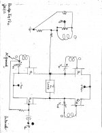
F6 with symmetric input
Hi,
i have all parts for my f6, i will start with the unbuffered version driven my my rtp3 preamp.
anyone tried to modify with a symmetric input?
my idea is to use positive phase of regular input and neg phase input from secondary feedback connection.
or can i use only one primary, but then i will loose 6db gain according my transformer know how?
thanks
- Home
- Amplifiers
- Pass Labs
- F6 Amplifier