Another suggestion to troubleshoot is to disconnect the negative feedback connection at the output. Load the output with a dummy resistor as a voltage offset may develop due to a possible mismatch of JFETs. Repeat your earlier measurements and observations.Excellentt buzz. Good tone. Firing her back up now. Let the entertainment begin.
Dont have gate stopper on 2sk170 CCS feeding my output bias LED's. Could this be it. suspect crappy wiring job, but we will see.
.....
moi suspect crappy mess ( even if it's always like that , even messier , with my ikebanas )
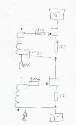
connect top of lower bias net (JfetCCS) to GND , instead to output
I can't see organization of GNDs on your pic , so it seems that you're on your own regarding that
be sure that repeaters aren't swallowing mains xformer field
Another suggestion to troubleshoot is to disconnect the negative feedback connection at the output. Load the output with a dummy resistor as a voltage offset may develop due to a possible mismatch of JFETs. Repeat your earlier measurements and observations.
there is no servo function of FE , with or without NFB
offset will stay the same , with or without NFB , with or without FE
Thanks ZM. Great points.there is no servo function of FE , with or without NFB
offset will stay the same , with or without NFB , with or without FE
ZM. Some of your concerns plagued the old classic design. Post #1085 page 3 of link; supplementary notes.moi suspect crappy mess ( even if it's always like that , even messier , with my ikebanas )
connect top of lower bias net (JfetCCS) to GND , instead to output
I can't see organization of GNDs on your pic , so it seems that you're on your own regarding that
be sure that repeaters aren't swallowing mains xformer field
Will its real absence cause buzz? lhquam's earlier circuits may have oscillated at low frequency with low values of these capacitors.Buzz,
Cap is missing across your bottom biasing circuit. ( second PDF)
Zen Mod. Can one operate [with signal] the output stage without negative feedback [open loop] and without a load to ground? Will this damage the JFETs?
it's possible to damage them only if you exceed their Ugs limit ;
chance for that are small - requires idiot driving insane voltage in input
chance for that are small - requires idiot driving insane voltage in input
SemiSouth R100 variability
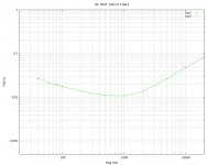
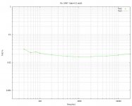
In my previous post http://www.diyaudio.com/forums/pass-labs/216616-f6-amplifier-147.html#post3156418 I show significant THD differences between 2 PC boards I built. Today, I swapped R100 output JFETs between boards (that was easier than swapping transformers). Here is THD vs Frequency of one of the boards, before and after the swap.
This indicates that there is considerable variability between the SemiSouth R100 JFETs. I do not know if it is input capacitance, transconductance, or something else.
Attachments
...connect top of lower bias net (JfetCCS) to GND , instead to output...
not seen this one but yes.
Two mistakes in the shematic but may be not in the circuit.
This indicates that there is considerable variability between the SemiSouth R100 JFETs.
Bad news
dunno
but , if made as drawn , lower Jfet can't be biased

Cap is on bottom section as well. Lower Bias network is not attached to ground at top but output. Everything biases perfectly, but i suspect ZM is right, its the tangled mess. Thats what i figured from beginning, as it was thrown together. I will rebuild and retest.
By mistage, the output voltage may reach power rails [and stick] as one JFET opens and the other simulatneously closes; like a switching or clipping situation. Will it affect [damage] the bias circuitry, and especially will this cause DC to flow through the secondaries [and primary].it's possible to damage them only if you exceed their Ugs limit ;
chance for that are small - requires idiot driving insane voltage in input
At 20kHz 1watt, the RMS AC gate current is about 40uA. I would expect leakage currents to be much lower than that. I seem to recall measuring the gate current as about 2uA when biased for 1.3A drain current. I did that measurement for only one R100 JFET.probably different gate leakage
Yeah, I was thinking the same. I am trying to order some non-A R100s right now from Newark.Wondering if the R100A parts are showing their colors vs their non A counterparts.
- Home
- Amplifiers
- Pass Labs
- F6 Amplifier