My understanding is that b grade is recommended.
and that matching is desirable.
Possibly from what you have match and pick the highest idss.
and that matching is desirable.
Possibly from what you have match and pick the highest idss.
A grade are low Idss for the F6.
Measure and label each Jfet, and use pairs wit the highest Idss you have. 6.0+ should work well. The circuit is designed for Idss around 8.0, but a few mA either way will still work.
Measure and label each Jfet, and use pairs wit the highest Idss you have. 6.0+ should work well. The circuit is designed for Idss around 8.0, but a few mA either way will still work.
So i can use grade A transistors without any problem or not? ... But better to match them to lowest difference as possible, finally two parameters lowest idss and lowest difference of each other. Correct?A grade are low Idss for the F6.
Measure and label each Jfet, and use pairs wit the highest Idss you have. 6.0+ should work well. The circuit is designed for Idss around 8.0, but a few mA either way will still work.
Another question.
How about make an expiriment with swapping Nichicon FG with Elna Slimic II?
Any benefits that we can measure? Or that just depends at mine ears?
Thanks also 6L6 and other members, for detailed explaination for each situation 😉 Very nice that you help to another members of community!
Last edited:
You can use the A jfet, just use the highest Idss pairs you can make.
Use whatever capacitors that make you happy. I like both the FG and the Silmic II. Expectation bias will make more of a sound difference than the actual materials.
Use whatever capacitors that make you happy. I like both the FG and the Silmic II. Expectation bias will make more of a sound difference than the actual materials.
6L6, something in this circut critically depends on that idss must be around 6.0 mA (that give mostly by grade B) or i can use transistors with 2.5 mA idss (grade A) without any problem? I mean circut designed espicially for grade B or that all depends on money at mine pocket? Thanks!
The circuit is designed around an Idss of about 8.0
6.0 should still work. 10.0 should still work.
2.5 is VERY low and you will have issues.
Again, you can use the A jfet, just use the highest Idss pairs you can make.
6.0 should still work. 10.0 should still work.
2.5 is VERY low and you will have issues.
Again, you can use the A jfet, just use the highest Idss pairs you can make.
The circuit is designed around an Idss of about 8.0
6.0 should still work. 10.0 should still work.
2.5 is VERY low and you will have issues.
Again, you can use the A jfet, just use the highest Idss pairs you can make.
Thanks, clear enough! 🙄
You can use the A jfet, just use the highest Idss pairs you can make.
Use whatever capacitors that make you happy. I like both the FG and the Silmic II. Expectation bias will make more of a sound difference than the actual materials.
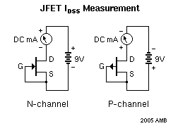
Hi...
I think this testrig is easier for everybody ?
I made this .pdf because i allways forget howto match them 😱
Jesper.
Attachments
Do not sleep the whole night, but i run 2 channels!
Nothing blow up, but sound that out of my speakes are plastic, and also looks like that sound position are different that must be. I hear that tonal balance are very good, for example on Sinatra voice, but i can't say that it's have "stereo scene", maybe on few tracks on my collection, of course two channels working, but i can't say that them work together to deliver 3D experience.
Anyone know what the problem?
Also LSJ74A - pair with idss 5,63 mA and 5,68 mA.
LSK170A - 6,44 mA and 6,46 mA.
And thanks for schematics for idss measurement, i saw that picture before via google.
Do not sleep the whole night, but i run 2 channels!
Nothing blow up, but sound that out of my speakes are plastic, and also looks like that sound position are different that must be. I hear that tonal balance are very good, for example on Sinatra voice, but i can't say that it's have "stereo scene", maybe on few tracks on my collection, of course two channels working, but i can't say that them work together to deliver 3D experience.
Anyone know what the problem?
Also LSJ74A - pair with idss 5,63 mA and 5,68 mA.
LSK170A - 6,44 mA and 6,46 mA.
And thanks for schematics for idss measurement, i saw that picture before via google.
Hard to say what the problem is.
Download ARTA and make some measurements with your computer soundcard.
Also post pictures, what you have done.
Hello here Pass_people 🙂
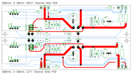
Anyone care to comment on my layout, specialized for my old all-aluminium/cobber chassis.
Board(s) are like the Diyaudio store boards "matched" left/right.
Transformers are Reichenbach's
Jesper.
Anyone care to comment on my layout, specialized for my old all-aluminium/cobber chassis.
Board(s) are like the Diyaudio store boards "matched" left/right.
Transformers are Reichenbach's
Jesper.
Attachments

Last edited:
Hello here Pass_people 🙂
Anyone care to comment on my layout, specialized for my old all-aluminium/cobber chassis.
Board(s) are like the Diyaudio store boards "matched" left/right.
Transformers are Reichenbach's
Jesper.
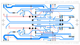
Not the worst PCB, but
in theory you could take the feedback from the output terminal and not from the transistor drain.
Not the worst PCB, but
in theory you could take the feedback from the output terminal and not from the transistor drain.
Hi... Thank's for answer! But i honestly can't see that?
Jesper.
Attachments
Hi... Thank's for answer! But i honestly can't see that?
Jesper.
I think you should be able to see how the R3 is connected to the output, just like the neg.ch output FET is connected to it and just like the source resistor of the pos.ch. is connected to it.
Other things you could consider:
You could try to closely couple all the flows and returns on the PCB (look at the transformer here),
try to minimise all the loop areas (input and feedback for example),
you could make the output stage pos.ch and neg.ch track impedances as low as possible and symmetrical
and you could make an ideal low impedance audio reference ground point where all audio returns connect.
That should make your PCB as invisible as possible to the circuit itself.
But your PCB is not a disaster, it is probably as good as the store board.
Which is "good enough".
You could try to closely couple all the flows and returns on the PCB (look at the transformer here),
= try to minimise all the loop areas (input and feedback for example),
==> That should make your PCB as invisible as possible to the circuit itself.
So if I infer from that: the routing of the signal through the capacitors should go on the other layer and run over the earth line, just having a bump where there is any solder point of that earth.
Ever heard of Oliver Heaviside? "Most of the energy runs not on and through the lines [PCB traces] but through the isolation and earth underneath". Well I reformulated it myself but gives us the thinking of a pioneer.
Every engineer talkf about inductance loops . oops
Every engineer talkf about inductance loops . oops
Then - - by looking through the print, you cannot see the trace anymore.
palstanturhin, thanks for commenting on my pcb... I will see how it will work. But as when you wrote, i alleready have drilled holes and everything on my raw pcb boards 🙂
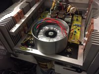
Anyway, i see that shielded torrid is prefered. But buying an new one, that is not going to happen!
I will try this stainless steel ring around my torrid for a start, and see if i will succes with that. Maybee put/welder a lit on it ?
That torrid, have been used in this chassis for both F4, AlephJ and the F5 which is sitting there now without noise/hiss ?
Jesper.
EDIT :: I just found this description of some fine torrid's 😛
Attachments

Last edited:
New toy.

First THD at 1000mA bias (1kHz/1W/8R) = 0.020%, not too bad...?
2nd and 3rd harmonics nice and even. No other harmonics.
Still lots to do to make it perfect though...
NE5534 preamp,
diamond buffer, (BC550/560, BD137/138)
LL1540
BD135 drivers
IRFP140 outputs
Me like!
Palstanturhin
Did you use the RC network and any R as per datasheet recommendation?
http://www.lundahl.se/wp-content/uploads/datasheets/1540.pdf
Cheers
Did you use the RC network and any R as per datasheet recommendation?
http://www.lundahl.se/wp-content/uploads/datasheets/1540.pdf
Cheers
Shorted Output
Hey, putting this out there just for reference to anyone that experiences a short.
I lent out a mosfets F6 to a friend. He said he shorted the output with large "audiophile cable spades". Luckily, only a few parts were fried.
The input transformer and jfets were not affected. Pleasantly surprised.
Obviously burnt were the source and drain resistors. The 100 ohm 3w resistor was OK, but changed it anyway. One of the gate resistors was reading weird in circuit, but ok outside- replaced it anyway. Only change 7 parts.
1k uF caps were ok.
Most parts tested ok in circuit, like resistors, zeners and caps. Saved time removing and testing them. I think the power resistors acted like fuses. Maybe their demise prevented other parts from burning. The 2.5 slo-blo fuse did not blow.
Brought everything up with a variac and it biased up nicely.
Maybe situation could have been worse, but that was my experience.
- Home
- Amplifiers
- Pass Labs
- F6 Amplifier