Pardon me for novice question, will R125 work with F6?
Papa used both types in his original J2 amps and declared that he treats them as the same.....🙂

Has any one tested the F6 sound with and without P3 & P4 trimmers?
Right now I’ve got P4 turned all the way clock wise and P3 just a touch from being all the way anti-clock wise. That leaves Q2 seeing 10 ohms from P4 and Q1 seeing about 0.2 ohm from P3.
It’s second harmonic and I do like it, but if I were to pass the P3&4 and the R13&14 all together, how would that change the sound – anyone know or have an educated guess?
ZM,
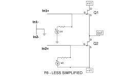
I'm about to test this bufferless balance F6 schematic you posted on #3086. Reason is a have a balance TVC with <100ohm pre-amp driving into balance TVC so the TVC output impedance is pretty low under attenuation, mid point. Anyone else tried this approach?
I'm about to test this bufferless balance F6 schematic you posted on #3086. Reason is a have a balance TVC with <100ohm pre-amp driving into balance TVC so the TVC output impedance is pretty low under attenuation, mid point. Anyone else tried this approach?
coffee is brewing , now ... so take this with grain of salt
schm from #3086 was just one of typical ZM's brainfarts

you have some later ones , confirmed in LTSpice and later in vivo (mostly by speedy guys in US of A)
sorry , I don't have exact links - either here or in some other F6 related thread
you have some later ones , confirmed in LTSpice and later in vivo (mostly by speedy guys in US of A)
sorry , I don't have exact links - either here or in some other F6 related thread
ZM,
I have search for it but only found balance input and balance output version.
Anyone else can point me to the right post? Many thanks in advance
Alex
I have search for it but only found balance input and balance output version.
Anyone else can point me to the right post? Many thanks in advance
Alex
aha
I also forgot that we didn't fiddle with bal in , SE out
just feed it with SE , making bal/se conversion prior to amp input
there is no benefit in over-complicating things , when you're anyway going to make it somewhere in chain
I also forgot that we didn't fiddle with bal in , SE out
just feed it with SE , making bal/se conversion prior to amp input
there is no benefit in over-complicating things , when you're anyway going to make it somewhere in chain
ZM,
My setup is balance output from Behringer to my balance input TVC with balance output. So I guess I need to hook up the - output to gnd since the TVC output is floating anyway, I can do that.
Alex
Sent from my C6903 using Tapatalk 2
My setup is balance output from Behringer to my balance input TVC with balance output. So I guess I need to hook up the - output to gnd since the TVC output is floating anyway, I can do that.
Alex
Sent from my C6903 using Tapatalk 2
Just share, i power up my F6 today with pot turn so initial current will be very low and as i slowly turn bias and offset pots up, i found that i could not get idle current to go beyond 1.3A and the Vgs measured 1.1xxV fr both top and lower JFET. Expect since Teabag labeled them as match Vgs 1.23V
I used 2 blue LEDS so i knew it wasn't a problem with not enough reference voltage. So i poke around and found there was almost 5V drop across R6 and about 0.5V across R5 (reference to variable second harmonic schematic in FW F6 article). So 2 things, first looks like for same Vgs, gate current vary significantly from sample to sample 0.5mA vs. 0.05mA and second I didn't quite expect the gate current to be so high. Looking at the datasheet they do claim Igs to be 10mA at Vgs of 2.6V so 0.5mA at 1.1xxV might be reasonable.
So for those of you who claim you could not get Vgs or Ids to 1.5A measure voltage across R5 and R6. Meanwhile i plan to change my R6 from 10k to 4.7k to double the available Iqs. I wonder if the Jensens transformer would tolerate a 1mA net DC current passing through its secondary?
Alex
Papa,
I have triple check cap polarity, its a brand new Elna Silmic II. Any issues with marching ahead with leaky JFET?
Alex
I have triple check cap polarity, its a brand new Elna Silmic II. Any issues with marching ahead with leaky JFET?
Alex
I just brain stormed how it would be possible to realize the P2-pot from the PLH to tweak the symmetry in this circuit:
So the in practice it would probably look like a F2 on top of another F2, and to incorporate feedback I think the easiest way would be to use one F6-transformer for each input so we can combine the output to the inputs, unless you can do it without the transformer that is.
The idea would be to have two separate input channels for the amp and use DSP to act as the P2 pot. The simple way would be to just reduce one side, or you could reduce and lowpass one side and all-pass the other for a more complex pattern. I think I have the wrong polarity on one of the inputs but with DSP that would be easy to change 😉
So my question is: is this completely crazy or is it something that actually could work?
Attachments
Papa,
I have triple check cap polarity, its a brand new Elna Silmic II. Any issues with marching ahead with leaky JFET?
Alex
what's voltage across R7 and R8 ( output gate resistors)
ZM,
Voltage across the 0.1IBM output degeneration resistors was about 0.13V but would not go further down. Output offsets was trimmed to within +/-0.05 Thats when I started to check Vgs etc
Alex
Sent from my C6903 using Tapatalk 2
Voltage across the 0.1IBM output degeneration resistors was about 0.13V but would not go further down. Output offsets was trimmed to within +/-0.05 Thats when I started to check Vgs etc
Alex
Sent from my C6903 using Tapatalk 2
Mighty ZM,
Voltage across R7 = 2.1mV, R8 = 21.9mV. I used 47.5Ω for R7 and R8 so current going into SS is Q1 is ~44uA and Q2 is ~460uA. Will change R6 to 4.7kΩ, that should double available gate current.
Alex
Sent from my C6903 using Tapatalk 2
Voltage across R7 = 2.1mV, R8 = 21.9mV. I used 47.5Ω for R7 and R8 so current going into SS is Q1 is ~44uA and Q2 is ~460uA. Will change R6 to 4.7kΩ, that should double available gate current.
Alex
Sent from my C6903 using Tapatalk 2
I have triple check cap polarity, its a brand new Elna Silmic II. Any issues with marching ahead with leaky JFET?
If it's that leaky, you have to replace it.
Historically I have now see a few failures where the Gate of the JFET gets
blown. These days I am protecting them with a 9.1V zener (nominal value)
just like Mosfets. Could be random failure, but I have noticed that none
with a Zener have died yet.
😎
- Home
- Amplifiers
- Pass Labs
- F6 Amplifier