Whilst carrying out the bias on a mono f5t, P1&P2 have run out of travel(25 turns)@ approx .2 v across TP2/TP3.
All the resistor values checked as per bom.
I am sure I have seen this situation previously, but cannot find the source.
rail voltage 32.5
R25/R26/R27/R28= 10k
R3/R4 read 48.6mv & 47.6mv, with P1/P2 at zero
All the resistor values checked as per bom.
I am sure I have seen this situation previously, but cannot find the source.
rail voltage 32.5
R25/R26/R27/R28= 10k
R3/R4 read 48.6mv & 47.6mv, with P1/P2 at zero
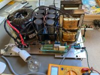
Which heatsinks did you use? Where to buy them?I`m also getting my parts in for an F5t V3 build. Rail voltage will be around 45 VDC, for R25, R26 33k and for R27, R28 10k will be used. PSU will be CLC using 44 mF 10 mH 44 mF per rail, so 352 mF in total. Two 800 VA torodials with 33 VAC secundaries. I`m heading for 0,6 - 0,64 A bias per device. Since I use a case with 4 bigger heatsinks for a stereo Build, I should end up with 55 - 56 C according to my calc. If it gets hotter I plan to reduce to 3 pairs of mosfets instead of 4 or I might use fans to get the amp below 55 degrees. the diodes will be used too, as you can see on the pics. Wish me luck! 😃
View attachment 1417637
With R25/27 & R26/28 at 10k/10k there should be around 16.25v on the cascode emitters (to GND) going to the JFETs.
(Rail voltage / (R25 + R27)) X R27
(32.5/(10+10)) x10 = 16.25v
Are you using 2SK/J BL or LSK/J B JFETs? Check R3,4 are 10R? You should be seeing around ~80mv across R3 and R4 (~8ma). Right now there's only 48-49mv (<5ma). You may need to add in the second pair to have enough current to drive the MOSFETs.
Check P1,2 R5,6 R11,12 and TH1,2 for correct values. (5k 1k 2.2k and 4.7k respectively)
Of course check all solder joints and Q1,2 & Q7,8 are in correct positions/orientation.
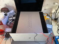
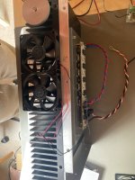
Walter, the heat sinks are sold by Fischer Electronics and actually for some reasons I still cannot set bias to the level I wanted. One reason is that the mosfet`s are sitting to close together on the pcb I`m using though I use a heatspeader the heatdistribution is not as even as it should be. So I have to use forced cooling. Nevertheless, I would not build such a monster 👹 again. I recommend to go with mono blocks. Everything will be easier, cable rooting, the chassis is cramped, the WEIGHT ( we talk about over 100 lbs in my case…) and so on. I consider my amp as a kind of engineering sample. Still have to improve the cabeling, as you can see on the pics. Will see where it will lead me. Maybe I use 4 pairs and forced cooling or simple reduce to 3 pairs naturally aspiered. 🙂 which might be sufficient anyway. Had it up and running, bias set to 0,570 A per device, which gave me around 60°C in the center of the two heat sinks at 21°C room temperature. Playing Dave Bruebeck on my Klipsch Forte, BA3 Preamp and Pearl 3 Phonopre. That was really nice! 🤪😛🔥
Attachments
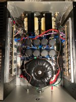
I built a similar F5Tv3 about 12 years ago. Pictures from March 2013, you can most probably find in this thread or the F5Tv3 thread. My problem was without a heatspreader that I couldn't get the temp off of the big MOSFET's down enough, so I made a kind of bar with M5 bolts so I could push the MOSFETS with big pressure to the heatsinks. But monoblocks are way better for this amp.


You used the same pcbs as I can see. Very nice built.👍
I`ll check for the temperature distribution between the mosfets on the heat spreader. Maybe there is also an issue. Thnx for the hint!
I`ll check for the temperature distribution between the mosfets on the heat spreader. Maybe there is also an issue. Thnx for the hint!
Hello ndiyer,
you could also lower the bias since you have around 50°C on the heatsinks...
Cheers
Dirk
you could also lower the bias since you have around 50°C on the heatsinks...
Cheers
Dirk
Yes, that is a solution to stay cooler. Forced cooling is already installed and I‘ll try different bias settings and conduct listening sessions to see what setting I like most, or if I can hear any difference at all. 🙂 Cheers
Last edited:
HiWith R25/27 & R26/28 at 10k/10k there should be around 16.25v on the cascode emitters (to GND) going to the JFETs.
(Rail voltage / (R25 + R27)) X R27
(32.5/(10+10)) x10 = 16.25v
Are you using 2SK/J BL or LSK/J B JFETs? Check R3,4 are 10R? You should be seeing around ~80mv across R3 and R4 (~8ma). Right now there's only 48-49mv (<5ma). You may need to add in the second pair to have enough current to drive the MOSFETs.
Check P1,2 R5,6 R11,12 and TH1,2 for correct values. (5k 1k 2.2k and 4.7k respectively)
Of course check all solder joints and Q1,2 & Q7,8 are in correct positions/orientation.
Cascode emitter (to GND) =15.1v,
JFET's are 6-8 mA, Diy Audio Store,
R3/R4 read 48.6mv & 47.6mv, with P1/P2 at zero,
All components checked for orientation and to BOM,
All joints reflowed,
Could I try 8-11mA JFET's
Hello
I have the pass 5 Turbo v2 and a problem. After I had the amplifier with an input signal and without a speaker at the output in operation, the right channel failed and outputs only a weak signal. The heatsinks on the right side also got cold. At the output I then measured an offset of more than 1 volt.
What can be the cause of the failure and which components can be damaged or what to do?
Thank you
Torsten
Torsten -
Since you say it's an F5t v2, this means no diodes and 36v rails. Yes?
Are the JFETs on the input boards cascoded, should be with 36v rails.
What is the bias for the MOSFETs you adjusted them to, check the left channel with input shorted?
Is the bias stable or does it vary as you watch the DVM? If so, how much?
What is the left channel offset with input shorted and no load?
Is the offset stable or does it vary as you watch the DVM? If so, how much?
Following the installation of 8-11mA JFET's,Whilst carrying out the bias on a mono f5t, P1&P2 have run out of travel(25 turns)@ approx .2 v across TP2/TP3.
All the resistor values checked as per bom.
I am sure I have seen this situation previously, but cannot find the source.
rail voltage 32.5
R25/R26/R27/R28= 10k
R3/R4 read 48.6mv & 47.6mv, with P1/P2 at zero
R3/R4 now read 76mV and 74mV,
Amplifier biasing as normal.
Many Thanks for all the help and advise,
Here are pictures of f 5. The set value was 350mv stable on both sides. The offset is still stable at 0.01mv on the left side. A mosfet is removed and measured and is okTorsten -
Since you say it's an F5t v2, this means no diodes and 36v rails. Yes?
Are the JFETs on the input boards cascoded, should be with 36v rails.
What is the bias for the MOSFETs you adjusted them to, check the left channel with input shorted?
Is the bias stable or does it vary as you watch the DVM? If so, how much?
What is the left channel offset with input shorted and no load?
Is the offset stable or does it vary as you watch the DVM? If so, how much?
Attachments

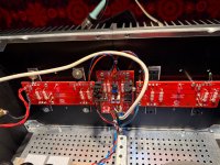
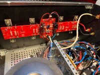
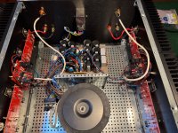
The set value was 350mv stable on both sides.
I found 350mV bias with the diodes is on the edge, I prefer 300 - 320mV, although many say higher bias sounds better.
You have the thermisters touching the metal washer on your MOSFET's, they only have a thin coating of paint on them and are known to cause issues. Move them so they touch the plastic case of the MOSFET's, see if that helps the channel come back to life.
One last thing, if you have no input, then no load is OK. Whenever I have an input, I make sure to have an 8 ohm load connected to the speaker terminals.
Thanks for the info. I will try it and report.
Are the capacitors C1x and C2x both 10uf necessary?
These have not yet been installed.
Are the capacitors C1x and C2x both 10uf necessary?
These have not yet been installed.
Are the capacitors C1x and C2x both 10uf necessary?
Yes, they are needed for rails above 24v.
- Home
- Amplifiers
- Pass Labs
- F5 Turbo Builders Thread