Hi all. I’m having a hard time translating the balanced turbo schematic to actual boards and hookups. If I take an input board and rotate it 180 degrees, like in picture below, I can’t reconcile it with Nelson’s template in Turbo article. Connections that I understand are as follows: XLR pin 1 will connect to both input board grounds, pin 2 will go to IN+ and pin 3 will go to IN-. I also understand OUT+ and OUT-. What I don’t understand is left side voltage and fets orientation. Which output board N or P goes top left and does it connect to + or - voltage? And all leftside fets on input and output boards are reverse of right side schematic, meaning left side shows Pchannel 2SJ74 in same position as where right side Nchannel 2SK170 appears, but that does not correlate with Nelson balanced template which has Nchannel in both top positions and both Pchannel in bottom position on schematic. What is correct and should fets be installed differently on left side input and output boards? Really confused and would appreciate any insights. Elwood625? Starcat? Anyone? Thank you!

Or is it as simple as building two regular stereo sides (output board-input board-output board) and making the proper xlr input connections, link between input boards, and +/- out?

Speaker - Output is normally connected in this configuration to the two positive Speakeroutputs
Or is it as simple as building two regular stereo sides (output board-input board-output board) and making the proper xlr input connections, link between input boards, and +/- out?
Speaker connections for this schematic has one input board and the two output boards connect to speaker positive, and the other input board and two output boards connect to speaker negative.
The XLR input has Pin 2 going to the input board for speaker + and Pin 3 going to the input board for speaker negative. Pin 1 goes to ground on BOTH input boards. Don't forget the "link" connection/wire that goes to connect both input boards.
Set P3 to halfway, when it's time for bias and offset, you will need DVOM's for:
1 - total offset between speaker positive and speaker negative.
2 - Offset for speaker positive to ground.
3 - Offset for speaker negative to ground
4 - Across source resistor for bias measurement
5 - Across the source resistor on the other output board.
Adjust one input board/output boards at a time, either speaker positive or speaker negative. I used 7 DVOM's so I could monitor both speaker positive and speaker negative just in case adjusting bias/offset on one input board doesn't make a change on the other. Bias and offset stability are EVERYTHING to prevent smoke/sparks. Keep a fire extinguisher handy at all times.
Bias adjust is the same as F5 and/or F5t, wait 1 hour after initial adjustment and make sure bias doesn't fluctuate. If offset is unstable, (can't keep the offset below 10mV), then you need to increase the gate resistor value for each MOSFET. Stay below 320mV for bias (without diodes) and 300mV with diodes. until you are positive offset and bias are stable. Then you can either add the diodes with bias at 310mV or go to 350mV without diodes, watch the heat sink temp.
This is how I built mine according to the Balanced turbo schematic.
The above wiring fault rectified.Ref #9,923
Took another look !
this photo reveals my issue
In the word of Captain Mainwaring "Stupid Boy"
Many Thanks Jim.
Back to the beginning.
Not able to achieve minimum resistance from P1.
P1 replaced, zero achieved at P1.
2v achieved across R5 R6, after 5 1/2 turns of P1 P2.
offset apparent after 8 turns of P1 &P2.
P1 increasers the offset, however further turns of P2 is ineffective at zeroing the offset.
I am concerned that I may have further damage as a result of my wiring fault.
Please may I have advise.
I have completed my Turbo build. I left out the "turbo diodes" since they may cause difficulty in setting the bias safely. I installed the 1000pF caps for C3 and C4. I implemented the 'lag resistors' as per Nelson's recommendation in post #3943. Bias is set at just shy of 0.300volts across the Test points and offset is zeroed. Everything seems to be working fine.
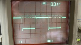
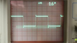
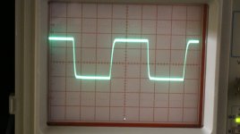
My question is regarding the square wave performance as seen on the Oscillogram below. There is a significant overshoot on the leading edge of the signal at the output. The square wave is 10Khz. The overshoot seems to increase as the power level is increased. Will this fry my tweeters?!! The frequency does not change when I increase or decrease the Square Wave frequency. Should I be concerned?
My question is regarding the square wave performance as seen on the Oscillogram below. There is a significant overshoot on the leading edge of the signal at the output. The square wave is 10Khz. The overshoot seems to increase as the power level is increased. Will this fry my tweeters?!! The frequency does not change when I increase or decrease the Square Wave frequency. Should I be concerned?
Attachments
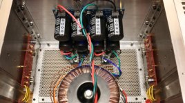
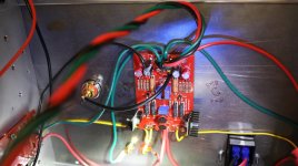
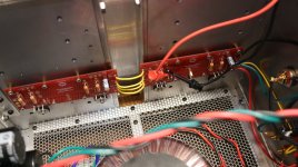
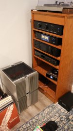
A couple of pics of the build. Heatsinks are 10" tall by 2-3/8" deep. Amps are monoblocks and are HEAVY! Transformer is Antek AU7434. PSU uses 22000 uF capacitors. 1Khz sine wave clipping is just over 82 volts P-P. Calculates to about 100 watts into my 8.25 ohm test load. Note the lag resistors are surface mount types near the cascodes in the picture. I cut the trace and stripped back the red lacquer to solder them in.
Attachments
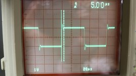
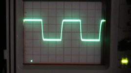
I found on page 14 of the F5 Turbo article a reference to using compensation caps across the feedback resistors to reduce oscillation. So I installed 1nF caps on R7 and R10. the overshoot is reduced but not gone. Am I chasing an inconsequential rabbit hole? First picture is before, second is after adding comp. caps to feedback resistors. Overshoot seems to be reduced by about half.
Attachments

Maybe try a larger value cap. You can get 2, 3, 4 nF and try the different values until the leading edge starts to roll off a bit. If you have 4 of the 1nF caps, you can even take them and parallel two on one channel for testing.
Am I chasing an inconsequential rabbit hole?
This is a quote from Nelson, I can't remember the the post#:
F5 turbo cascading:
Apropos of cascoding the F5 Turbo front end:
Since the original, playing with this sort of circuit and with different devices and
such, I decided that there is astability advantage to having some resistance
off the Drains ofthe input devices when cascoding. This means 100 to 200
ohms (or so) between the Drains and the Emitters of the cascode transistors.
I have seen several examples of cascoded F5's tend toward oscillation, often
fixed by a lag resistor (Drain to Gate) on the outputs, but traceable to the
low impedance seen by the input device Drains (the Cascode).
How to:
Lift the Emitter, bend leg forward.Solder resistor to end of leg.
Bend resistor underneath leg,Heat-shrink and bend resistor lead down into Emitter pad.
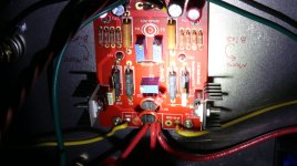
Thanks. I installed 150 ohm surface mount chip resistors by cutting the traces on the boards and stripping away the red paint to create solder pads. they hardly show up in the pictures. I'm learning that my camera sometimes prefers manual focusing... I'm going to order some 2n2 and 3n3 caps soon and try those in the locations listed earlier to see what effect they have. It will be a couple of weeks...
Can someone tell me will the matched jfets 8 to 11 ma be fine , I am renewing my f5 turbo amplifier
^ See link below. Relevant information copied and pasted. I believe, but am not certain, that this information came from Nelson Pass.
https://diyaudiostore.com/pages/idss-choice
https://diyaudiostore.com/pages/idss-choice
- F5T V1,2: 6-8 mA (operated at Idss - 1 mA)
- F5T V3: 8-11 mA (operated at Idss - 1 mA)
After Action Report.
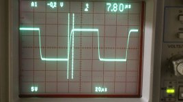
10Khz 500mV square wave input to the amps after tweeking the compensation caps... 131 is first amp, 132 etc. are 2nd amp. Ended up with 1nF across the resistors R7 and R10. P-channel boards required 2-3300pF caps, one on each board. N-channel boards required 2-2200pF caps, one on each board. the cascode resistors were left in. P3 is centered. The sound, driving B&W 801 S2 Matrix speakers and sourced by Shanling Et3 through Eversolo DMP-A8 Sounds WONDERFUL! Like live music! I'm listening to "Audiophile Analog Collection" Vol.1 and its WOW! Everything is revealed, even the dropped mic cable...
Thanks Nelson and everyone who made this possible.
Attachments

So I was told I could use the 8ma or 11ma jets , cascode amp. Can someone tell me what the 8 vs 11 difference is in this application.
- Home
- Amplifiers
- Pass Labs
- F5 Turbo Builders Thread