Hi there,
Beginner here, so I could use all the help I could get 🙂
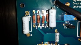
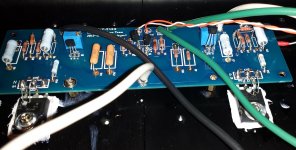
I started building my F5.. Power supply tested good. So I fired on with a dim bulb attached. The bulb lit for a second or 2 and dimmed completely but I saw some smoke coming out of R19 and R20... Here is a picture where you see R20 discolored 😱 ... any advice before I do more damage😀
Edit: One channel attached, I have not yet assembled the other board. The short ti,e it was up, I read 0V across R11 R12
Thanks
KJ
Beginner here, so I could use all the help I could get 🙂
I started building my F5.. Power supply tested good. So I fired on with a dim bulb attached. The bulb lit for a second or 2 and dimmed completely but I saw some smoke coming out of R19 and R20... Here is a picture where you see R20 discolored 😱 ... any advice before I do more damage😀
Edit: One channel attached, I have not yet assembled the other board. The short ti,e it was up, I read 0V across R11 R12
Thanks
KJ
Attachments
Last edited:
Hi Zen Mod,
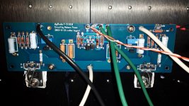
I am using the "official" F5 build (schematics) with 2SK170, 2SJ74, IRFP9240, IRFP240, ZTX550 and ZTX450 ... I followed the pinout on the board using the build guide as a reference - on page 13, they gave the pin orientation of the different parts that can be used for the build.
Here is another picture, maybe someone more knowledgeable like yourself will spot what I am doing wrong 🙂
Thanks
KJ
Attachments
why JFets are backwards ?
also bjts are looking backwards
and left NTC is dangerously close to mosfet washer , with naked legs
also bjts are looking backwards
and left NTC is dangerously close to mosfet washer , with naked legs
Last edited:
Reverse Q6 like ZM mentioned. Can't see Q5 but it's probably the same.
Q1, Q2 are also reversed, why ?
Rgds,
Eric
Q1, Q2 are also reversed, why ?
Rgds,
Eric
Last edited:
well - OP didn't read build guide enough times 😉
check Jfets just in case ( common Idss test with 9V battery and mAmeter)
replace them if needed , even if I believe that they're good
replace small bjts without hesitation
replace R19 and R20
triple check pinout of parts prior to powering up ....... post pic here , so we can check together
check Jfets just in case ( common Idss test with 9V battery and mAmeter)
replace them if needed , even if I believe that they're good
replace small bjts without hesitation
replace R19 and R20
triple check pinout of parts prior to powering up ....... post pic here , so we can check together
Thank you Eric and ZM,
I will recheck/reposition Q5 Q6 and report back... also push NTC away from the washer.
Thanks again
I will recheck/reposition Q5 Q6 and report back... also push NTC away from the washer.
Thanks again
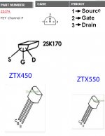
As FYI to other extreme newbies like me, here are the pinouts for Q1 Q2 Q5 and Q6 (2SK170, 2SJ74, ZTX550, ZTX450)
I am going to fix the mess and will post the picture here before powering as ZM suggested in case I do another monumental mistake 🙁
Thank you again gentlemen for your help
KJ
I am going to fix the mess and will post the picture here before powering as ZM suggested in case I do another monumental mistake 🙁
Thank you again gentlemen for your help
KJ
Attachments
Hi,
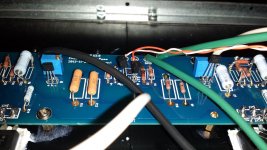
I turned around the transistors (replaced ZTXs and resistors). Does the board look ok now? Can I go ahead and power it on?
PS. I will probably replace the whole board but I want to make sure that it's fine the way it is so I do not waste another pcb/parts
Many thanks
KJ
I turned around the transistors (replaced ZTXs and resistors). Does the board look ok now? Can I go ahead and power it on?
PS. I will probably replace the whole board but I want to make sure that it's fine the way it is so I do not waste another pcb/parts
Many thanks
KJ
Attachments
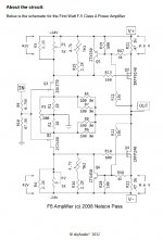
Thanks Eric... before I do that, I did some googling and double checked the resistors value and the ones I am using (from the BOM - for board rev 2, I am using rev 3 - are 100R) but the ones on this schematics posted by 6l6 on the F5 board thread are 10k? Actually there are other differences, for instance the schematic shows R21 and R22 as 2.21k while in the BOM they are 10k. Are versions 2 and 3 of the board using different schematics/versions of the F5?
If someone could clarify this to me, I would greatly appreciate it.
Thanks
KJ
If someone could clarify this to me, I would greatly appreciate it.
Thanks
KJ
pinout looks good now
regarding resistors :
resistor going from ztx base to rail - 100R
resistor going from ztx base to output - 10K
I'm sure you can decipher which ones they are
regarding resistors :
resistor going from ztx base to rail - 100R
resistor going from ztx base to output - 10K
I'm sure you can decipher which ones they are
No don't fire it up ! You have all the resistors in the wrong places. I see they have renumbered all the resistors on the version 3 .0 boards.
i.e. R5 - R8 from V2.0 is now R9-R12 on V3.0 boards
i.e. R5 - R8 from V2.0 is now R9-R12 on V3.0 boards
Well I have bigger problems then... the resistors are not the right value...R19 and R20 should be 10k and I am using 100R ! I was following the wrong schematic all along. In the attached schematic from the pdf guide, R19/R20are 100R 🙁 ... like I said in my other post, there are other differences in the values... can you please confirm that 6l6 schematic I linked to is the right one for the store board version 3? Many thanks
Attachments
Thanks WalterW, I think you are right. I should use the schematics from the 5FT article where Nelson Pass talks about the F5 first before talking about the changes for the Turbo version.
Actually it's all written on the board page in the store... I should have paid more attention to the change log... unfortunately the Schematics button on the same page links to the one for board version 2!
V3.0
Change to F5 schematics from F5 Turbo article
Minor diagram change in NTC and limiter sections
P3 added to adjust N/P variations to reduce distortion
Relabelling of resistors to match schematics
Last edited:
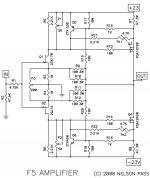
yep, I checked. The schematic I posted is the right one for the V3.0 boards.
It is from the F5 turbo article with the addition of P3. I have both v2.0 and v3.0 boards here so it was easy to check.
So all resistors, except R13 and R14, seems to be wrong...
It is from the F5 turbo article with the addition of P3. I have both v2.0 and v3.0 boards here so it was easy to check.
So all resistors, except R13 and R14, seems to be wrong...
- Status
- Not open for further replies.
- Home
- Amplifiers
- Pass Labs
- F5 build power on with smoke from R19 and R20