It was supposed to be similar to the one you posted (#962), have I missed something? Or are you just saying that the capacitor could do with being larger (and I wouldn't disagree although overall loop feedback will tend to flatten this out anyway, same as for the bias spreader resistors as discussed previously).
How do you get an opamp that will handle the common-mode voltages on the inputs without having its voltages shifted close to the rail. Then the problem is with the opamp output voltage swing.
I'm finding that LTSpice is sometimes even dumber than me
rest of time is normal , I'm dumber
rest of time is normal , I'm dumber
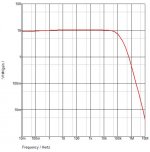
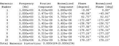
This variation of post #962 simulates very well. It has 6.4mA/C OS bias current variation per degree C variation and 3.5mV/V OS bias current per volt rail voltage variation. The distortion is amazingly low, even at 100W with 2R load. Cascode transistors were omitted from the schematic for simplicity, but were present in the simulations.
Attachments
yeah
with our splitting da hair , we each came to simply ridiculous circuit behavior
have no doubt that builds will be successful
hopefully soon
with our splitting da hair , we each came to simply ridiculous circuit behavior
have no doubt that builds will be successful
hopefully soon
When using two optocouplers, one for each drain sense resistor, must the optocouplers always have at least one direct common connection between their transistors? Such as the emitter of one opto directly connected to the other opto's collector, or emitter to emiter.

Yes, totally ridiculous.
1kHz 8R 1W 5W and 25W
1kHz 8R 1W 5W and 25W
.step watts=1
Fourier components of V(out)
DC component:0.00303776
Harmonic Frequency Fourier Normalized Phase Normalized
Number [Hz] Component Component [degree] Phase [deg]
1 1.000e+03 4.200e+00 1.000e+00 -0.32° 0.00°
2 2.000e+03 1.499e-06 3.568e-07 -14.41° -14.10°
3 3.000e+03 3.647e-06 8.684e-07 89.18° 89.50°
4 4.000e+03 3.043e-09 7.246e-10 -157.83° -157.52°
5 5.000e+03 9.179e-09 2.186e-09 -35.57° -35.25°
Total Harmonic Distortion: 0.000094%(0.000000%)
.step watts=5
N-Period=4
Fourier components of V(out)
DC component:0.00305182
Harmonic Frequency Fourier Normalized Phase Normalized
Number [Hz] Component Component [degree] Phase [deg]
1 1.000e+03 9.392e+00 1.000e+00 -0.32° 0.00°
2 2.000e+03 7.579e-06 8.070e-07 -14.26° -13.94°
3 3.000e+03 4.222e-05 4.496e-06 89.26° 89.58°
4 4.000e+03 7.254e-08 7.724e-09 177.94° 178.25°
5 5.000e+03 6.289e-07 6.697e-08 -89.14° -88.82°
Total Harmonic Distortion: 0.000457%(0.000000%)
.step watts=25
N-Period=4
Fourier components of V(out)
DC component:0.00310534
Harmonic Frequency Fourier Normalized Phase Normalized
Number [Hz] Component Component [degree] Phase [deg]
1 1.000e+03 2.100e+01 1.000e+00 -0.32° 0.00°
2 2.000e+03 4.675e-05 2.226e-06 -11.56° -11.24°
3 3.000e+03 5.937e-04 2.827e-05 89.32° 89.64°
4 4.000e+03 6.711e-06 3.196e-07 178.52° 178.84°
5 5.000e+03 6.098e-05 2.904e-06 -90.83° -90.51°
Total Harmonic Distortion: 0.002851%(0.002603%)
1kHz 2R 100WFourier components of V(out)
DC component:0.00303776
Harmonic Frequency Fourier Normalized Phase Normalized
Number [Hz] Component Component [degree] Phase [deg]
1 1.000e+03 4.200e+00 1.000e+00 -0.32° 0.00°
2 2.000e+03 1.499e-06 3.568e-07 -14.41° -14.10°
3 3.000e+03 3.647e-06 8.684e-07 89.18° 89.50°
4 4.000e+03 3.043e-09 7.246e-10 -157.83° -157.52°
5 5.000e+03 9.179e-09 2.186e-09 -35.57° -35.25°
Total Harmonic Distortion: 0.000094%(0.000000%)
.step watts=5
N-Period=4
Fourier components of V(out)
DC component:0.00305182
Harmonic Frequency Fourier Normalized Phase Normalized
Number [Hz] Component Component [degree] Phase [deg]
1 1.000e+03 9.392e+00 1.000e+00 -0.32° 0.00°
2 2.000e+03 7.579e-06 8.070e-07 -14.26° -13.94°
3 3.000e+03 4.222e-05 4.496e-06 89.26° 89.58°
4 4.000e+03 7.254e-08 7.724e-09 177.94° 178.25°
5 5.000e+03 6.289e-07 6.697e-08 -89.14° -88.82°
Total Harmonic Distortion: 0.000457%(0.000000%)
.step watts=25
N-Period=4
Fourier components of V(out)
DC component:0.00310534
Harmonic Frequency Fourier Normalized Phase Normalized
Number [Hz] Component Component [degree] Phase [deg]
1 1.000e+03 2.100e+01 1.000e+00 -0.32° 0.00°
2 2.000e+03 4.675e-05 2.226e-06 -11.56° -11.24°
3 3.000e+03 5.937e-04 2.827e-05 89.32° 89.64°
4 4.000e+03 6.711e-06 3.196e-07 178.52° 178.84°
5 5.000e+03 6.098e-05 2.904e-06 -90.83° -90.51°
Total Harmonic Distortion: 0.002851%(0.002603%)
Harmonic Frequency Fourier Normalized Phase Normalized
Number [Hz] Component Component [degree] Phase [deg]
1 1.000e+03 1.050e+01 1.000e+00 -0.34° 0.00°
2 2.000e+03 5.852e-04 5.573e-05 179.54° 179.89°
3 3.000e+03 4.249e-06 4.046e-07 -134.08° -133.74°
4 4.000e+03 1.963e-04 1.869e-05 178.58° 178.92°
5 5.000e+03 8.890e-05 8.467e-06 88.66° 89.00°
Total Harmonic Distortion: 0.005939%(0.005838%)
Lynn, you also had another design on post #1077 that sounded very promising. What happened with that design?
Lynn, you also had another design on post #1077 that sounded very promising. What happened with that design?
Funny that you asked that. I revisited that design yesterday and tried more tests did not like some of its behavior. Another downside is the greater complexity and component count.
Well, from looking at some of your older posts on how to check phase margin it looks like the circuit in post #1077 has a negative phase margin. That is if I did the test correctly, the circuit is a bit different then your examples.
This variation of post #962 simulates very well. It has 6.4mA/C OS bias current variation per degree C variation and 3.5mV/V OS bias current per volt rail voltage variation. The distortion is amazingly low, even at 100W with 2R load. Cascode transistors were omitted from the schematic for simplicity, but were present in the simulations.
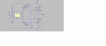
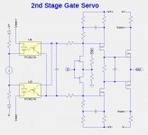
This circuit is very similar to one I published in post #1326 which has good servo control so I am not surprised that yours performs well too. Apart from the obvious servo implementation specifics, I note that you are using only overall loop feedback. I’m guessing that this is why the distortion is so low, i.e. a lot of global feedback is being employed. I’ve said it before but I will say it again, my concern here is around stability. How does the circuit perform with a square wave input?
This aside, what is your thinking in including source resistors in the 2nd stage MOSFETs, albeit bypassed by the capacitor? Given that this stage is included in the servo loop, it should be perfectly fine (and simpler) to omit both the resistors and capacitors.
A practical difficulty I found with my variation is that the bias of the 2nd stage and output stage is now tightly coupled which makes for some difficulty in setting up the circuit in practice, i.e. setting the pots properly and choosing the right value of the resistor between the 2nd stage MOSFET drains. I also wonder whether it is really ideal to have a change in output stage current, say due to temperature, impact the front end bias as it must with this type of circuit.
Finally, an obvious point but worth making perhaps? Including the output stage bias resistor between the 2nd stage MOSFET drains will mean that the front end cannot swing close to the rail voltage (the bias voltage is effectively subtracted). Placing the servo control between the output stage gates overcomes this problem due to the action of the capacitors.
I’m thinking that if we wish to control the bias of the front end without using (bypassed) degeneration, we may well be better off using two servos, i.e. similar to the concept of ZM’s post #1314, one for the front end and another for the output stage.
- Home
- Amplifiers
- Pass Labs
- F4 Beast Builders