so , when it will be tried?
I have these mostly populated ....... but few more urgent things to do before
The simulations I did today did not pass your pulse tests. Lots of tweaking is required and I am not sure it will be a winner.
...
Quote:
Originally Posted by lhquam
Have you tried anything like this? You might thing PSRR is a problem, but PS variations and noise are mostly common-mode to the diff-amp.
naah
name of the game is to avoid using Arduino or 486 for biasing circuit , so no go 🙂
...

That circuit shown in post #1313 was an idea from 15 months ago that I never fully simulated then, but I did more simulations yesterday and it might be something to seriously consider. The (minimum) peak detector for the summed FET currents is a really good way to measure the bias current. This is based on the FET Id vs. Vgs equation being something like a square law, and
The challenge with the rail-to-rail resistor divider circuit is to replace to diff-amp opamp and buffer with some sort of simple circuit, preferably not needing +15/-15 power.

I have no doubt it'll work , when polished
however ..... any iteration I tried and was satisfied with performance , was too complicated for my liking
that one from post #1314 is least complicated one , of which I am satisfied with functionality
OK , Babelfish is title of necessary complicated iteration of Papa's , so it's customary to complicate , but too much is just not satisfactory ...... world is full with good amps , but just small number of them is elegant
and Old Devil is more than enough experienced to know when erring on side of elegancy is not loosing in functionality
and yes , I lost looooong time ago count of how many iterations I tried , at least half of them calling - final ........
...
and Old Devil is more than enough experienced to know when erring on side of elegancy is not loosing in functionality
and yes , I lost looooong time ago count of how many iterations I tried , at least half of them calling - final ........
...
Papa is the wizard at designing low component count circuits with excellent performance.
And I also have gone through many design iterations, most of which are really too complicated with little or nothing to be gained over the recent "improved" opto circuits.

My experience sounds similar to both of yours ZM and Lynn. The difficulty is not in coming up with variations but in doing so with simplicity and having it work well.
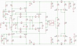
I too have played with many versions and in the spirit of sharing attach the one I found to work best, consistent with not being too complicated. It is not ideal though and I like the look of the latest dual opto solution with zeners more and intend to try it out, i.e. build it.
I too have played with many versions and in the spirit of sharing attach the one I found to work best, consistent with not being too complicated. It is not ideal though and I like the look of the latest dual opto solution with zeners more and intend to try it out, i.e. build it.
Attachments
I'm fed up with PL/FW simplicity
from now on , I'm only building ML knockouts ..... and will make a fortune !!

from now on , I'm only building ML knockouts ..... and will make a fortune !!
price is going exponentially with every additional part
symmetrical Widlar with 50 transistors,minimum ......... etc.
🙂
symmetrical Widlar with 50 transistors,minimum ......... etc.
🙂
...
I too have played with many versions and in the spirit of sharing attach the one I found to work best, consistent with not being too complicated. It is not ideal though and I like the look of the latest dual opto solution with zeners more and intend to try it out, i.e. build it.
I like that one. The only problem might be that the cascodes are loaded by the 240R load resistors to the rails, vs. 33k(+/-) resistors with the output fet bias spreader servo. You need to estimate or measure in SPICE the open-loop-gain of that bias servo. It might be lower than the servo on the output FET gates.
I haven't measured the servo open loop gain but it seems to adequately compensate for changes in output stage current so I don't believe it to be an issue. Actually my motivation for connecting the servo as shown is so that it also works to control the bias of the front end MOSFETs.
My experience appears to differ from yours here in that I find the FE MOSFET current drifts without source resistors. I'm wondering now whether it might be better to keep the source resistors and bypass them at AC with capacitors either directly to the power rails or perhaps to a point somewhere along the cascode resistors as you have shown previously. The latter appears to have the potential advantage of a better low frequency response if the point is chosen carefully.
Thoughts?
Ian: Thinking about it more, the difference in connecting the opto output to the nodes between the JFETs and the cascode BJT emitters vs. connecting between the cascode BJT collectors is the voltage across the opto output transistor. Vce is limited to 30 volts or so on most optos, so the cascode connection solves that problem.
Look at post #962 F4 Beast Builders....
My experience appears to differ from yours here in that I find the FE MOSFET current drifts without source resistors. I'm wondering now whether it might be better to keep the source resistors and bypass them at AC with capacitors either directly to the power rails or perhaps to a point somewhere along the cascode resistors as you have shown previously.
...
Thoughts?
Your point Lynn? I've seen this before and it is what I was referring to by connection "to a point somewhere along the cascode resistors". Are you saying that this is your preferred approach?
I forgot to mention that the above approach has the potential issue that the DC value across the capacitor can be quite close to zero. Consequently it may be necessary to use a non-polarised type which are not that common in the large values needed in this application. Not a show stopper but maybe there is a better way?
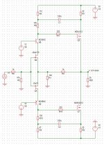
In the schematic in post #962, the AC component of Vgs of the j313 and k2013 FETs is not affected by the value of the (DC degeneration) resistor from source to rail, other than ESR (parasitic internal resistance) of the cap. Connecting optos as shown in that schematic makes use of the lowpass filter formed by RC network involving the electrolytic.
ESR and RC time constant are serious problems if you use the simpler circuit which bypasses the source resistor with a large electrolytic. For instance if you want a 47R source resistor for DC degeneration and a time constant of 1 second you would need a 20mF capacitor. You actually need a much longer time constant to keep AC degeneration to a acceptable level. I actually built an amplifier using that circuit but its performance suffered from ESR problems with the caps.
You can safely run electrolytics slightly reverse biased without problems.
Last edited:
I did both a "back of the envelope" estimate and a simulation check of the current gain from the cascode collector to the j313 drain, ie. d(Id(Q5))/d(Ic(Q6)) in your circuit in post #1326. The estimate takes the form R8*gm(Q5) = 240R*.23S = 55x, assuming Id(Q5)=36mA. That means an opto servo connected between the cascode emitters has about 35dB more open loop gain than one connected between the output stage gates. That surprised me.I haven't measured the servo open loop gain but it seems to adequately compensate for changes in output stage current so I don't believe it to be an issue.
...
In the schematic in post #962, the AC component of Vgs of the j313 and k2013 FETs is not affected by the value of the (DC degeneration) resistor from source to rail, other than ESR (parasitic internal resistance) of the cap. Connecting optos as shown in that schematic makes use of the lowpass filter formed by RC network involving the electrolytic.
ESR and RC time constant are serious problems if you use the simpler circuit which bypasses the source resistor with a large electrolytic. For instance if you want a 47R source resistor for DC degeneration and a time constant of 1 second you would need a 20mF capacitor. You actually need a much longer time constant to keep AC degeneration to a acceptable level. I actually built an amplifier using that circuit but its performance suffered from ESR problems with the caps.
You can safely run electrolytics slightly reverse biased without problems.
I agree with you regarding simple bypass of the source resistor although I haven't actually tried it in this particular circuit.
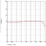
Regarding the other form as per your much earlier post, I am not so sure about the source resistor only providing DC degeneration. As you say, there is a filter function at work here and depending on the value of the capacitor, this will impact the low frequency response (open loop). See the attached by way of example.
Call me a belt and braces man but I prefer not to run electrolytics with any kind of reverse bias although you are quite likely correct 🙂
Attachments
- Home
- Amplifiers
- Pass Labs
- F4 Beast Builders