Very good question.Sorry, I wasn't sufficiently clear. I meant the output stage as shown does not have a response down to DC. The capacitors C3 and C4 become ineffective and the resistors R14, R12 and R15, R13 act as potential dividers so that there will be some attenuation at DC. All a bit theoretical perhaps but a real effect surely?
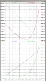
The left plot in post #1293 does not indicate the behavior you are predicting. To make sure that I wasn't seeing something weird in SPICE AC Analysis I did the following tests. The tests were to measure the p-p V(Out) at 1kHz and 1mHz, with and without the C1, C2 caps. Here are the numbers.
25W with C1 C2
20kHz 40.3583
1mHz 40.3463
25W without C1 C2
1kHz 40.3474
1mHz 40.3457
I am not sure I understand why we see this behavior. Perhaps the bias servo maintains the "proper" difference between the FET gates and the global feedback maintains the output offset near zero even without any caps. The net result is that the voltage difference across the 10K resistors stays the same.20kHz 40.3583
1mHz 40.3463
25W without C1 C2
1kHz 40.3474
1mHz 40.3457
what about discrepance (I would say , almost customary) between dissipation figure of 120W/ch and (leaked) value for Iq?
Baaad Papa!
🙂
Baaad Papa!
🙂
How much of the idle power dissipation goes to power supply inefficiencies, the FE, and the OS? I estimate about 4W/ch for the FE. What is the power supply efficiency? If the power supply dissipates 32W, then 100W/ch is available for the OS. 100W/80V = 1.25A for 40V rails. Perhaps the rail voltages are lower with the 0R17 sense resistors.what about discrepance (I would say , almost customary) between dissipation figure of 120W/ch and (leaked) value for Iq?
Baaad Papa!
🙂
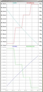
What effect will a sag of that magnitude have on the sound of the amplifier?
Probably a lot less than the effect on the ears that listened to the tone
burst at full power for 1 second.
I think I figured out what is really going on. In order to obtain the effect that you predicted the open-loop-gain (OLG) of the front-end must be lower than 1e4 that was used in the previous simulations. Here are the peak-to-peak output voltages with and without C1 and C2, and at 3 different values of OLG. With high values for OLG, the output offset correction by feedback through the FE centers the FE output offset to the average of the FET gate voltages.Sorry, I wasn't sufficiently clear. I meant the output stage as shown does not have a response down to DC. The capacitors C3 and C4 become ineffective and the resistors R14, R12 and R15, R13 act as potential dividers so that there will be some attenuation at DC. All a bit theoretical perhaps but a real effect surely?
1kHz 25W 8R
Cf OLG Vpp(Out)
0 1e2 35.6273
0 1e3 35.6273
0 1e4 40.3477
3.3mF 1e2 36.6278
3.3mF 1e3 39.988
3.3mF 1e4 40.3583
Cf OLG Vpp(Out)
0 1e2 35.6273
0 1e3 35.6273
0 1e4 40.3477
3.3mF 1e2 36.6278
3.3mF 1e3 39.988
3.3mF 1e4 40.3583
I agree. I was talking about open loop behaviour where the response is about 6dB down without C1 and C2. Sufficient overall feedback will indeed compensate for this though I don't know whether it is desirable.
Of course we will want the capacitors for other reasons too, e.g. to smooth the output from the servo and to allow the front end to swing almost rail to rail peak voltage which otherwise it cannot do. Of more interest is how to determine the proper values of capacitor. Larger values will give less low frequency reduction for the front end to compensate but I wonder whether the large time constant may give rise to issues with the bias voltage, e.g. small signal following a pulse? I believe Nelson is still using 220uF even in the XA25 but of course I could be wrong.
Of course we will want the capacitors for other reasons too, e.g. to smooth the output from the servo and to allow the front end to swing almost rail to rail peak voltage which otherwise it cannot do. Of more interest is how to determine the proper values of capacitor. Larger values will give less low frequency reduction for the front end to compensate but I wonder whether the large time constant may give rise to issues with the bias voltage, e.g. small signal following a pulse? I believe Nelson is still using 220uF even in the XA25 but of course I could be wrong.
I’ve finally figured out how the forward biased Zener approach works. Call me dumb as it took longer than I feel it should.
Coincidentally or otherwise, the Zener appears to have exactly the effect I was trying to achieve with my earlier posting which didn’t work very well. In summary, it acts to limit the bias servo such that bias stays constant once the output stage current reaches 2 x the bias current, i.e. as one of the output devices begins to switch off. This observation provides the necessary clue as to how to calculate the proper values for the various resistors.
The Zener also improves the sensitivity to changes in output stage bias current as you have noted. This is more obvious in terms of how it works as it simply replaces the variable voltage drop due to current through Ropto1 for a fixed value.
How to calculate Ropto1? In simple terms, it needs to be chosen such that the voltage drop across it and the Zener are equal to 2 x output stage bias current at idle. Smaller values are preferred to maximise sensitivity but the choice is constrained by the small range of voltage drops obtainable from typical diodes. Rsen can also be adjusted if desired to assist in achieving the required result.
If the value of Ropo1 is off (too small or large), the bias voltage will exhibit either a sag or upward drift as you have observed. That said, I’m with Nelson in believing the audible impact of small changes here to be of little real consequence.
Rcs is much harder to calculate and will in case need to be a pot in order to adjust the bias current. The actual value will depend on many factors, including the values of R12 and R13, the CTR of the opto used and the voltage across the opto LED at the chosen current.
The optimum value of R12 and R13 is itself an interesting question as it appears to be a compromise between obtaining sufficient current through the optocouplers (smaller value) and power supply rejection (better with higher value). How did you choose your value of 33k?
I agree with much of what you said. I gave up trying to develop equations for the resistors because of the non-linearities of the diodes and LEDs making it difficult to determine the voltage drop for a given device current.
I use LTSpice operating-point sweeps of various parameters to search for usable parameter values. I then use sweeps of the rail voltage and temperature to determine the servo sensitivity to the parameter. I use a modified version of the schematic to compute the open-loop gain of the servo. Finally to run transient analysis, applying sin wave inputs of varying amplitudes, frequencies, and output loads to see the behavior of various waveforms.
I use LTSpice operating-point sweeps of various parameters to search for usable parameter values. I then use sweeps of the rail voltage and temperature to determine the servo sensitivity to the parameter. I use a modified version of the schematic to compute the open-loop gain of the servo. Finally to run transient analysis, applying sin wave inputs of varying amplitudes, frequencies, and output loads to see the behavior of various waveforms.
The diodes are performing two functions:I’ve finally figured out how the forward biased Zener approach works.
...
In summary, it acts to limit the bias servo such that bias stays constant once the output stage current reaches 2 x the bias current, i.e. as one of the output devices begins to switch off. ...
...
- voltage drop enabling Ropto1 to be reduced.
- on-off switch to stop conduction when reverse biased. This prevents LED saturation and
There is another aspect to the choice of Rcs. When properly chosen, the rail voltage sensitivity can be nulled. Theere are teo points where rail voltage variations affect the circuit: 1) the currents thru the 33k bias spreader resistors, and 2) the current thru Rcs. If you carefully examine the circuit you will see that increasing the rail voltages causes the currents thru the 33K resistors and Rcs to increase. The increase in current thru Rcs causes the current thru the opto LEDs and transistors to increase. The combined effect is the the current (changes) into the Drive+ and Drive- nodes have some degree of cancellation, depending of the values of the circuit parameters, particurly Rcs.
have we consensus about sense resistor being part of CRC in PSU filter ?
in other words - what ya say ?
in other words - what ya say ?
You might do that, but the hocky-pucks have low enough lambda (channel length modulation, or Early Effect) that the output FETs can be driven directly from the first stage of the CRC filter, and the second stage drives the Front-End.have we consensus about sense resistor being part of CRC in PSU filter ?
in other words - what ya say ?
The downside of of using the CRC resistor as a sense resistor is that all of the rectification noise between the 1st and 2nd caps appears across the sense resistor. Maybe that isn't so bad. Not sure.
Have you tried anything like this? You might thing PSRR is a problem, but PS variations and noise are mostly common-mode to the diff-amp....
FYI : I abandoned PL solutions , both with 0R47 and newer one with (supposedly) 167mR ; I believe we got it , in various ways , how Papa did it .... so , why not trying it in different way
...
🙂
Attachments
You might do that, but the hocky-pucks have low enough lambda (channel length modulation, or Early Effect) that the output FETs can be driven directly from the first stage of the CRC filter, and the second stage drives the Front-End.
The downside of of using the CRC resistor as a sense resistor is that all of the rectification noise between the 1st and 2nd caps appears across the sense resistor. Maybe that isn't so bad. Not sure.
will try ; me thinks that can't do any harm but ..... was dumb so many times before , once more will not change anything , except increase enjoyment
Have you tried anything like this? You might thing PSRR is a problem, but PS variations and noise are mostly common-mode to the diff-amp.
naah
name of the game is to avoid using Arduino or 486 for biasing circuit , so no go 🙂
you have (I believe ) last iteration of my CM based circuit ....... not really changed afterwards , except connecting driver sources pre-sensing resistor , not after
in fact , here it is ; central placed CCS is LT3092 helped with LT1634
as most things , it is a blatant exploitation of Papa's Breadcrumbs ..... but certainly way too far from real McCay , so no biggie posting it here
disclaimer - not yet confirmed in vivo
disclaimer two - it'll work , why not

Attachments
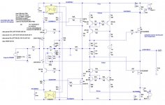
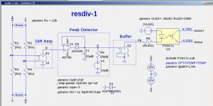
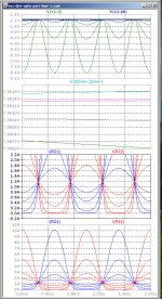
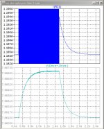
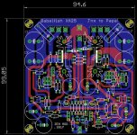
I did a very similar circuit to the JFET gates. Plots show J313/K2013 and OS FET currents vs temperature and rail voltage. I might have built PCBs for this amp.
Attachments


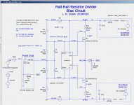
The circuit in post #1315 is very unusual because of the bias spreader. The servo adjusts the J313/K2013 bias, which in turn adjusts the voltages on the OS FET gates. A very small change in the FE bias will change in the voltage at points A and B and will result in a considerably larger change in the OS bias. Knowing the approximate OS gate voltages at the quiescent bias current allows the bias spreader resistors to be chosen for very good bias control of both the FE and OS. The quiescent OS bias is adjusted with the pots labeled RsenP and RsenN.
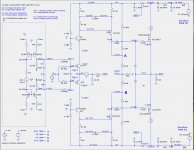
Here is a better version of the schematic with component values, voltages, and currents shown.
Here is a better version of the schematic with component values, voltages, and currents shown.
Attachments
- Home
- Amplifiers
- Pass Labs
- F4 Beast Builders