
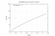
I think it is time for me to stop the simulations and build the beast. It is a waste of time to do more simulations when I do not even have a SPICE model for the IXFN48N60P which I am using in my build. My simulations have been based on the IXFN44N80Q3 because of the availability of a SPICE model from IXYS, but that FET has a much lower gm.
Hm... can you show a beast circuit that is stable with your criteria?
Looks like you already have something. Great work.
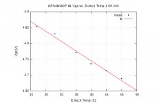
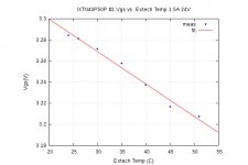
I have some measurement data for the IXFN48N60P.
Great.
These match my results exactly. (ie within 5%)
Yours are about 5% higher transconductance values.
I used 20V Vds not sure whether that would make a difference though.
Either way, 5% is really nothing.
Last edited:
It is interesting that the XA25 User Manual does not show plots of THD vs. Frequency or a plot of the residual distortion waveform. I am now getting THD figures close to those plots, but the H2 phase wanders all over the place. Maybe it is no longer important at such low distortion levels.
Nelson does this mostly in the FW manuals, but not in the Pass Labs products.
Here showing the distortion graphs for the XA25 is unusual.
Normally you have to wait for reviews to get these data!
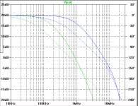
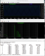
Pico: Here is how I create my Bode plots in LTSpice. The plots shown here, the Green trace is the AC Analysis with Amplifier input (ACIn) as the source, abd the Blue trace is with feedback input to the JFET stage (ACFB) as the source. I have not been able to improve the phase and gain margins much beyond what is shown here without reducing other performance parameters. The ACIn response looks pretty good to me, but the feedback loop could use some improvement. I estimate that the slew rate is at least 100V/us in the feedback loop, but only 12.5V/us w.r.t the Input.
Attachments
Last edited:
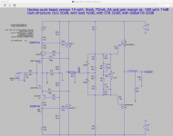
Indeed the circuit version ten I have running at home and showed here
http://www.diyaudio.com/forums/pass-labs/300233-f4-beast-builders-43.html#post4954633
shows a low gain margin at -180° look at the picture. Ugly peak in the higher region.
Nevertheless I never had problems in real life driving the amp the last week, thanks God!
Some months ago I tried some Goldmund clones and I had oscillation because the speaker cable was to near to the mains cable...... awful!
I am so happy that the FW builds are made in a way by Nelson that we do not have these problems!
Next posting my better version 14.
Attachments

Last edited:
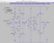
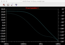
O.K. version 14. I tried to take the Sony II version 1 as model.
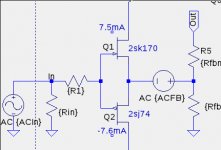
The gain margin is -14dB at -180° of phase. No more ugly peak.
You see the currents and gain structure in the picture!
Not yet playing, but soon!
The gain margin is -14dB at -180° of phase. No more ugly peak.
You see the currents and gain structure in the picture!
Not yet playing, but soon!
Attachments

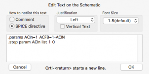
Gerd: In your simulations, insert a voltage source of 0V, with the the AC amplitude of 1 at the jfet feedback point shown in post #467. In my LTSpice simulations I do the following: .params ACIn=1 ACFB=1-ACIN .step param ACIn list 1 0 Then when you run the AC Analysis, you will get Bode plots w.r.t. the Input and the feedback loop, as shown in plot #467.


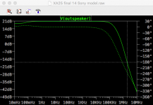
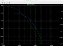
and this one goes up to 200kHz, I had to lower the 10k at the input to 4k7.
But here we do not have again the security margin of -12dB, IIIHHHH
But here we do not have again the security margin of -12dB, IIIHHHH
Attachments
Last edited:
I am assuming that the green plots are for ACIn and blue for ACFB. For ACIn there appear to be essentially zero phase and gain margins. For ACFB you have a rather interesting phase curve making both the gain and phase margins favorable. I need to examine the circuit more closely to understand what is causing that beneficial behavior.
Another observation. The ACIn Bode plot show that the ouput is -3dB at about 150kHz, and the ACFB Bode plot show the -3dB point only slightly higher. This is the result of relatively high MOSFET gate resistances and high impedances of the feedback network and the FE output load resistance.
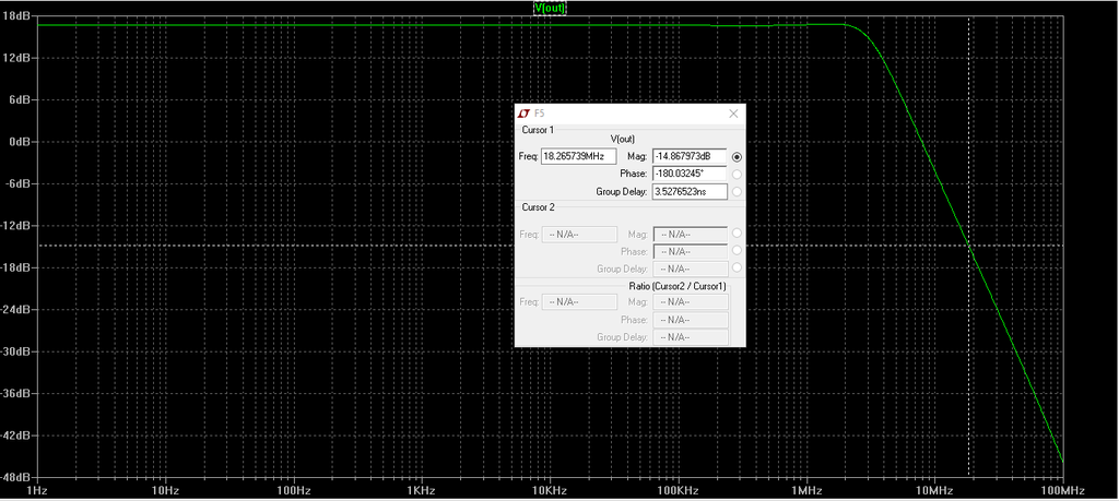
Here is an example measurement of F5 ie approximately -15dB at -180 degrees
Seems I got irritated by not switching off the right sidebar...
why are the sidebar values different from the phase degree values in the box.....
so irritating ......😱
but I learn....
hope the readers too, at least some.....🙂
- Home
- Amplifiers
- Pass Labs
- F4 Beast Builders