I can't solder directly to IC pin 16 (REF GND). There is a big ground fill that I soldered the two caps to that runs under the DAC IC and connects to pin 16; it also has vias to the bottom layer and is the best GND point.
C3 I started with 2.2uF X5R and REF was still noisy, so I went up to 100uF X5R 6.3V 1210 (you can use a 10V part but they are bigger and I didn't have any). Voltage coefficient of capacitance gives -10%.
Seriously, even the impedance along 4mm of 30AWG wire shows at this pin with my scope. It's some kind of nasty high-freq load with 20-100MHz switched cap transients. It's a great teacher
I've tried ceramic, tantalum, film, electrolytic and you need a mix. Still experimenting for best solution but people wanted to know what I was doing.
The inductor L1 is working "backwards"- you get more noise on the load side than on the +5VA supply side. Without it, some noise on pin 17 made it back to +VA. Because iron-core is no good here; using Dale/Vishay IM-10 and I don't like the SRF and am going to try a ferrite bead.
prairiemystic, since it sounds like an issue with killing the noise to the chip rather than increasing the available current, do you think a snubber would be appropriate here?
Nice work Prariemystic! There's all sorts of gremlins in that gigawork board due to the lack of a solid ground plane. DIP adapters are convenient for fiddling, but there's no substitute for getting the chips down on a good bunch of copper.
I laid out my own board for that reason. My prototype has those caps a bit farther away from the chip than I'd like. I used a film cap, a big ceramic and an even bigger tantalum for VREF and FILT+.
Sheldon
I laid out my own board for that reason. My prototype has those caps a bit farther away from the chip than I'd like. I used a film cap, a big ceramic and an even bigger tantalum for VREF and FILT+.
Sheldon
Good day 🙂
Friends, on which diodes you upgrade basic BYV26E?
Vishay 1N5062 will be a worthy replacement?
Thank you!
Friends, on which diodes you upgrade basic BYV26E?
Vishay 1N5062 will be a worthy replacement?
Thank you!
Good day 🙂
Friends, on which diodes you upgrade basic BYV26E?
Vishay 1N5062 will be a worthy replacement?
Thank you!
I find the BYV26 excellent "Fast Soft–Recovery Controlled Avalanche Rectifiers" trr=30 or 75ns. Pretty clean switching. I'd leave them in.
The 1N5062 is standard recovery, too slow trr=4us.
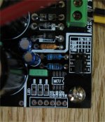
CS4398 VREF decoupling cap experiments
I had to stop working on the VREF decoupling cap experiments, the pcb can't take any more rework. I'm using an RF spectrum analyzer now. Harmonics run past 75MHz which rules everything out except for ceramic and mica.
For now, an inductor 47-100uH (less than 10 ohms DC) and 100uF X5R works excellent. Ferrite beads didn't cut out enough.
I find the BYV26 excellent "Fast Soft–Recovery Controlled Avalanche Rectifiers" trr=30 or 75ns. Pretty clean switching. I'd leave them in.
The 1N5062 is standard recovery, too slow trr=4us.
Thanks, I have understood! 🙂
Do I understand this right that I have to remove the 1k resistor on the undersideFor now, an inductor 47-100uH (less than 10 ohms DC) and 100uF X5R works excellent.
and cut the trace on top of pcb and inject the L1 at pin 15?
Last edited:
Do I understand this right that I have to remove the 1k resistor on the underside
and cut the trace on top of pcb and inject the L1 at pin 15?
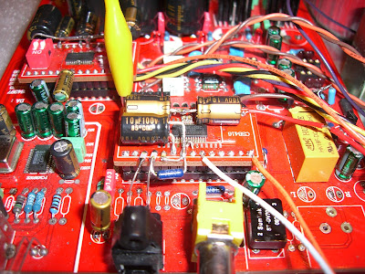
You replace the 1k ohm resistor that's located "in" the DIP socket, with an inductor. Then cut the skinny trace on the CS4398 DAC IC smurf board that runs from pin 15 to pin 28, right by the silkscreen outline. It's hard to see it and I use an ohmmeter to check things. Goal is for DIP pin 15 to now get +5VA via the inductor.
Thanks for your input...
A question
I've got this dac plugged into a WinXP machine via USB. I've noticed 2 things:
1) My volume slide in the OS doesn't work. The media player volume slider works. The OS volume slider works with my previous USB dac. Not so much this one.
2) This DAC seems louder to me than my last usb dac.
My dac came in an empty box, with no documentation. So I looked at the board and tried a jumper settings for USB operation, and I got sound to come out, so I left it at that. But now I wonder if I have it wrong, and that's why it doesn't respond appropriately to OS volume. I looked back at post 301 of this thread and saw some info on jumper settings, but with the various revisions to this board around I don't know if that info is still good. Could someone go over the current setup for input selection with me?
Attached: current jumper setting
Attachments
Hello,
I did not come here for more than 6 months when I stopped any tweak on this DAC.
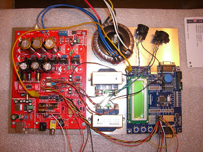
My latest mods was adding an external MCU for all software commands (both CS8416 and CS4398) and capacitors upgrades on the small boards for 8416 and 4398.
I did followed all the recommendation from receiver / DAC spec which was not there on original Gigawork design and I used NPO cap for the NP ones and Nichicon MUSE for the pol ones.
I also separated some power rails for analog / digital section decoupled by beads.
In the end it was a lot of effort mods for very little (none) improvement. 🙁
I believe to be efficient that the system needs a good new PCB layout with large grounding planes and the DAC / receiver on the main board.
The additional MCU board helped me to play with all the options through SPI interface (internal filters / PLL, input selection with button / remote control, electronic volume, mute,...).
I spent a lot of time there (not mentionning about transfo upgrades, ...) and in the end everything end up in a drawer after realizing the time spent vs. improvements...
It is just my experience... 😱

I did not come here for more than 6 months when I stopped any tweak on this DAC.
My latest mods was adding an external MCU for all software commands (both CS8416 and CS4398) and capacitors upgrades on the small boards for 8416 and 4398.
I did followed all the recommendation from receiver / DAC spec which was not there on original Gigawork design and I used NPO cap for the NP ones and Nichicon MUSE for the pol ones.
I also separated some power rails for analog / digital section decoupled by beads.
In the end it was a lot of effort mods for very little (none) improvement. 🙁
I believe to be efficient that the system needs a good new PCB layout with large grounding planes and the DAC / receiver on the main board.
The additional MCU board helped me to play with all the options through SPI interface (internal filters / PLL, input selection with button / remote control, electronic volume, mute,...).
I spent a lot of time there (not mentionning about transfo upgrades, ...) and in the end everything end up in a drawer after realizing the time spent vs. improvements...
It is just my experience... 😱
You replace the 1k ohm resistor that's located "in" the DIP socket, with an inductor. Then cut the skinny trace on the CS4398 DAC IC smurf board that runs from pin 15 to pin 28, right by the silkscreen outline. It's hard to see it and I use an ohmmeter to check things. Goal is for DIP pin 15 to now get +5VA via the inductor.
So the Vref gets +5 volts from 2 loations the 1k resistor and the skinny trace.
aint that strange? 😕
So the Vref gets +5 volts from 2 loations the 1k resistor and the skinny trace.
aint that strange? 😕
Yup, it's got something to do with the board supporting so many DAC IC's. The 1k on pin 15 is a pullup for the 'ol CS4397 MUTE, and watch the +/-12V at pins 17,18
 which is needed for the PCM1798 smurf board's op-amps. If someone actually put an IC in the socket (i.e CS4397) there would be s m o k e !
Well I just did the mod to set the LPF to Cirrus Application Note AN48 recommended values. Must say the DAC is better, smoother more analog sounding for it. It's a rather formidable DAC now 🙂 This is after I had earlier bypassed the buffer opamp stage and put in some of prairemystic's mods on the cs4398 board. Thanks for the ideas.
Wonder why the designer (Snow?) did not implement AN48 😕
Wonder why the designer (Snow?) did not implement AN48 😕
Alex_twn, your mods look really good. What is wrong with the sound? The main board grounding has a couple faults but not enough to make it sound poor.... In the end it was a lot of effort mods for very little (none) improvement. 🙁 I believe to be efficient that the system needs a good new PCB layout with large grounding planes and the DAC / receiver on the main board.
I note your transformers are big, which means they have big magnetization currents and I'm not sure the 'lil 4398 can do well there.
Hello,
I spent a lot of time there (not mentionning about transfo upgrades, ...) and in the end everything end up in a drawer after realizing the time spent vs. improvements...
I have few suggestions:
Instead of just randomly applying capacitors everywhere, it is better idea to actually measure the ground noise at various IC pins, and THEN play with capacitor types AND values. Desired outcome is drop in random wide spectrum noise. Where you solder those capacitors is also very important. Getting rid-off DAC and receiver IC sockets AND soldering the IC modules directly on to the PCB is another great improvement.
The DAC PCB is designed for 4397 (mine is!); so try to find this DAC IC plug-in module. 4398 implementation on this PCB is compromised and will never give as good results as with 4397.
Once you maxed the mods in the abovementioned areas, AND if you wish to do so, you could use external oscillator clock for the resampler / upsampler plugin module, if you decide to use the upsampler module of course. This oscillator will need completely separate, very low noise power supply AND will have to be grounded to a point on the DAC PCB with lowest noise.
Audio transformers should actually be bolted / screwed to a metal plate that sits at DAC PCB ground potential. You can keep the wood plate, just add large metal plate on top of it, and mount everything on this metal plate.
The controller board might be injecting huge amount of noise on to DAC PCB… (crocodile clips and long thin cable are not good solution to bring both PCB’s ground potential together).
Good luck,
Boky
Alex_twn, you're still having four electrolytic caps coupling the dac chip? Get rid of them and short the links. I found them to be one major bottleneck in the sonics.
2.5v dc
If you want to send 2.5v dc through along with the signal.Alex_twn, you're still having four electrolytic caps coupling the dac chip? Get rid of them and short the links. I found them to be one major bottleneck in the sonics.
- Home
- Source & Line
- Digital Line Level
- Experience with this DIY DAC ?