Is that more, less or roughly equal issue for current output versus voltage output DACs? Such as ES9038Q2M with I/V versus CS4398 voltage output and standard filter?
I would normally expect so.
Interestingly, it looks like what Cirrus did with CS4398 for the recommended output stage shown in the datasheet was keep all the time constants matched between the + and - outputs, but make the resistance levels much lower for the noninverting opamp input side. Maybe that was just to keep noise noise down where they could, maybe the opamp output wouldn't like it for the inverting side so they couldn't do it there.
Also, looks like the electrolytic cap to ground (in series with 487R) on the noninverting side before the opamp keeps the opamp from removing the dac output DC offset. Not sure why they did that. Then they had to use another electrolytic after the opamp for DC offset blocking. It might measure better that way due to some quirk of the dac chip outputs, but I would expect it to sound like there are electrolytics in the audio path. Kinda odd.
Can you tell what output stage topology they used in the EMU?
Last edited:
It does not look like they followed AN48. The extra electrolytic is not there.
Layout wise it has two electrolytic caps (both 47uF) placed between the CS4398 and the first dual op amp package. There is the official EVB (attached) but the physical location of the electrolytic caps in the layout does not seem to make sense for that circuit either. (Unless there are traces going the long route.)
Physically the layout locations seem to be something along the lines of:
CS4398 > 2x47uF > NJM2068 Filter > Relay (for -10 or +4 levels) > 2 More NJM2068 For Balanced Output
Attachments
I love my EMU 1616m. Take care of it, deserves.
And yes, I note those kind of differences between Left/Right CH, and between units (Dacs/ADCs)
I have done some similar restoration/ tweaking, good quality bypass caps, and in the 1 CH all opamps OPA1612..
Here it is the better pairing, at an optimum level.
(2nd at - 128dB, 3d at - 135dB)
And yes, I note those kind of differences between Left/Right CH, and between units (Dacs/ADCs)
I have done some similar restoration/ tweaking, good quality bypass caps, and in the 1 CH all opamps OPA1612..
Here it is the better pairing, at an optimum level.
(2nd at - 128dB, 3d at - 135dB)
Attachments

Not, no SMD film. Solid polymer electrolytics, different sizes and types, as they could fit in place (space is really restricted)
First I have done only the opamp swaps, and that gave a substantial improvement, most importantly at high freq range.
Then did the recapping, and was quite surprised when I saw thd going that low in the R channel..
A note: keep the series decoupling caps in place.
Thd crashes without them.
First I have done only the opamp swaps, and that gave a substantial improvement, most importantly at high freq range.
Then did the recapping, and was quite surprised when I saw thd going that low in the R channel..
A note: keep the series decoupling caps in place.
Thd crashes without them.
Has anyone ever managed to extract usable data from the on board controller?Reprogramming or replacing the onboard processor.
Last edited:
I love my EMU 1616m. Take care of it, deserves.
And yes, I note those kind of differences between Left/Right CH, and between units (Dacs/ADCs)
I have done some similar restoration/ tweaking, good quality bypass caps, and in the 1 CH all opamps OPA1612..
Here it is the better pairing, at an optimum level.
(2nd at - 128dB, 3d at - 135dB)
Wow, almost the exact changes I am in the middle of.
Can you give more information on the caps you used? I tried regular electrolytics and solid polymer for the ADC filter caps without a measured difference. (But stock opamps.) I also tried SEPC (OSCON) for the CS4398 filter cap but I got better measurements with Nichicon VR.
So I would love to know more about the vendor, series and values you used. And which were most critical to get the performance you measured.
Great. Thank you! I will try some of those.
To repair the power supply I used 1000uF 25V SAMYOUNG NXA 105C long lifetime low ESR capacitors.
To repair the power supply I used 1000uF 25V SAMYOUNG NXA 105C long lifetime low ESR capacitors.
Last edited:
Has anyone ever managed to extract usable data from the on board controller?
I think someone in this thread once dumped the I2C registers in order to address start up issues.
What people have done is monitor the I2C bus when the dac boots up and or when inputs are switched by moving jumpers. Capturing that data gave some clues to using the dac chip. However, now that ESS has opened up the datasheets we are free to talk about how to program the dac chip to do whatever. No longer any need to watch the dac board MCU do it.
Dimdim wrote somewhere that he could simplify the control program written for the ES9038Pro chip for the ES9038Q2M chip to fit in an Arduino Nano. If Dimdim doesn’t have time for that, maybe he can give someone else permission to do it so he doesn’t have to start from scratch.
IIRC Dimdim stated in other threads that anyone is free to use and or modify his ES9038PRO code to suit their needs. Again IIRC, the main complication is that he obfuscated the register data by hiding it in an EPROM. Now that ESS has made the data sheets public, the problem is to remove the EEPROM references and replace that with actual register data as required for the target dac chip.
Last edited:
I have been working on improving both the measurements and sound quality of my interfaces (which I have used to measure my ES9038Q2M experiments) and I have some questions regarding clocks and jitter.
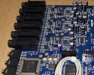
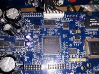
The first picture is from the E-MU 1616m which is the best measuring equipment I have right now for my DAC measurements. It has a very good JTest result in REW. The vendor appears to be TAI TIEN ELECTRIC for the two oscillators: CETGCG 45.158 and CETGCG 49.152 are the markings. E-MU describes it as an "Ultra-low jitter clock subsystem". I don't know if the Xilinx Spartan FPGA is part of the reason for the very good JTest results.
The second picture is from a Digidesign 003 rack which has much worse JTest results. This is disappointing for a number of reasons. Since this interface comes with CS5361 ADC which are pin compatible with CS5381 I had a number of planned uses for this equipment. (Not just making measurements.) Each oscillator consists of an HC-49 crystal, two caps, one resistor and one Philips/NXP 74HCU04D hex unbuffered inverter. Would this type of clock be expected to produce dramatically worse jitter?
I was thinking of making a small board with the CETGCG or similar oscillators and Micrel MIC5219 ultra low noise regulators to "upgrade" the Digidesign 003 rack clocks. (The MIC5219 are used for the E-MU 1616m DAC and the loopback looks very good as far as noise/absence of any spurs.)
Does this upgrade plan sound like a promising/sound approach?
I was thinking of removing the HC-49 crystals, caps and resistor and then inputting the new clock signal into the 74HCU04D input (which is pin 1 the way the crystal is connected).
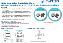
Edit: I don't know what series the "CETGCG" marked oscillators are, however I just found that TAITIEN makes low noise oscillators specifically for high resolution audio (at least that is what the datasheet says). That is the attached third image.
The first picture is from the E-MU 1616m which is the best measuring equipment I have right now for my DAC measurements. It has a very good JTest result in REW. The vendor appears to be TAI TIEN ELECTRIC for the two oscillators: CETGCG 45.158 and CETGCG 49.152 are the markings. E-MU describes it as an "Ultra-low jitter clock subsystem". I don't know if the Xilinx Spartan FPGA is part of the reason for the very good JTest results.
The second picture is from a Digidesign 003 rack which has much worse JTest results. This is disappointing for a number of reasons. Since this interface comes with CS5361 ADC which are pin compatible with CS5381 I had a number of planned uses for this equipment. (Not just making measurements.) Each oscillator consists of an HC-49 crystal, two caps, one resistor and one Philips/NXP 74HCU04D hex unbuffered inverter. Would this type of clock be expected to produce dramatically worse jitter?
I was thinking of making a small board with the CETGCG or similar oscillators and Micrel MIC5219 ultra low noise regulators to "upgrade" the Digidesign 003 rack clocks. (The MIC5219 are used for the E-MU 1616m DAC and the loopback looks very good as far as noise/absence of any spurs.)
Does this upgrade plan sound like a promising/sound approach?
I was thinking of removing the HC-49 crystals, caps and resistor and then inputting the new clock signal into the 74HCU04D input (which is pin 1 the way the crystal is connected).
Edit: I don't know what series the "CETGCG" marked oscillators are, however I just found that TAITIEN makes low noise oscillators specifically for high resolution audio (at least that is what the datasheet says). That is the attached third image.
Attachments
Last edited:
Dimdim wrote somewhere that he could simplify the control program written for the ES9038Pro chip for the ES9038Q2M chip to fit in an Arduino Nano. If Dimdim doesn’t have time for that, maybe he can give someone else permission to do it so he doesn’t have to start from scratch.
BuffaloDAC/ES9028 at master * possum64/BuffaloDAC * GitHub
Kozard,
You could try some good clock modules, but hard to say how much difference they might make in this situation. For good clocking, IME and IMHO, as with dac chips, implementation around the device matters a lot.
Wouldn't be surprised at all if NDK SDA clocks (still available from diyinhk) can outperform a clock made out of a crystal and some logic inverters. However, to get the best out of a clock: PCB design matters, power quality matters, decoupling matters, and clock signal distribution details matter. Buffering the clock output with a clock line driver device may be an important part of signal distribution for some use cases, and the buffer implementation would then matter too.
OTOH, simply wiring in a better clock than you have now could help quite a bit or it could turn out to be a failed experiment. IME clock modules are typically most stable when driving a simple nearby load, such as one dac. When driving a several dacs and ADCs, some kind of buffer would likely be needed, say, NB3L553-D (also well powered and decoupled). Whether buffers can be powered off the same regulator as the clock module driving them can be a tricky question. Again IME, it really depends on implementation details. Some experimentation may be needed.
EDIT: Regarding the Taitien clocks you referenced, they require decoupling much like the small Accusilicion AS318-B clocks do. For the latter a 402 size cap is needed within 1mm of the clock power pad, and with a direct trace going to the clock ground pin. If not decoupled to spec, the small AS318-B clocks may not work. The layout shown by Taitien on the sheet you attached shows a very similar arrangement. The other thing about Taitien clocks is that I don't know of a source for them, again much like the situation with small case size Accusilicon AS318-B. As a practical matter it seems NDK SDA or Crystek are the best audio clocks that are easy for diyer's to find (and with a good implementation they can actually be quite good). The last thing about clocks, again IME, is that they are most stable when left running constantly. If implemented that way, it adds some complication to the design.
Last edited:
bimo,
Thanks for the link. However, I think converting Dimdim's code to work with ES9038Q2M is mostly complete. Only a few minor bugs left was my casual impression.
The other issue of course would be the design of a good ES9038Q2M PCB. There has been some talk about it some offline, but its still too early to say what outcome there might be, if any.
Wouldn't be surprised at all if NDK SDA clocks (still available from diyinhk) can outperform a clock made out of a crystal and some logic inverters. However, to get the best out of a clock: PCB design matters, power quality matters, decoupling matters, and clock signal distribution details matter. Buffering the clock output with a clock line driver device may be an important part of signal distribution for some use cases, and the buffer implementation would then matter too.
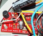
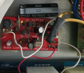
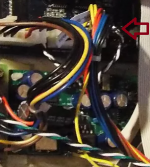
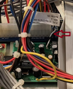
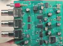
There is apparently a bit of an industry in existence which modifies/improves these recording interfaces. I have not been able to find the clearest pictures but I have attached images of:
- Image 1 & 2: Older (Digidesign 002 Rack) upgrade clock PCB (red).
- Image 3 & 4: Newer (Digidesign 003 Rack) upgrade clock PCB (green).
- Example external clock from the same vendor as the upgrade PCB.
So based upon this detective work I am hopeful it is worthwhile. I will look into the oscillators you mentioned and try to be extra careful on the regulator, layout, bypassing, etc.
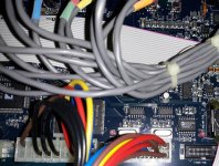
On two of the images I have placed red arrows showing the black and white wires which connect to the digital PCB. They appear to be going directly to the location of the HC-49 & 74HCU04D that I showed in my previous post.
Attachments
Last edited:
if you are thinking of making an external clock board, that would be one thing. Trying to put a new clock in the space where the old crystal and inverter stuff was located would be something very different.
If serious about clocking at all, I think you should get/borrow/etc. a 100MHz (or better) scope. Ideally get a low capacitance active probe for for the scope too, even a used ebay cheapie, maybe a P6201 with the set of slip-on attenuator probe tips (ground spring almost always missing from those probes so you might have to make one).
With at least some minimal test equipment so you can see what you are doing, and if wanting to build an external clock board, then I think you would have the best chance for a good result.
- Home
- Source & Line
- Digital Line Level
- ES9038Q2M Board