This is where machined 0.100" female molex headers come in handy. Just snip off a 3-some and you can swap to your heart's content.
Thanks. I've used this approach on other projects, but this is probably a really good time to use it again.
Jac
Power Layout
I have been making steady but slow progress on my EQ OPP build. This thread as been very quiet. Am I the only one actively trying to build this pre, or is everyone else just have fewer questions?
I have been thinking about the layout of the boards and their power wires. Of course, having regulated DC power and a good design for noise rejection should help, but I might as well use good practice and minimize any noise risk.
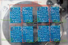
The boards are laid out such that you can't help crossing under the signal sections of the PCB. My current thought is to run power for the lower boards under the middle of the PCB where the CCS and tube live. Please see the photo for a rough idea. Red is power and green is signal.
I am open to ideas. You gents have much more experience with this than I do. I could shield the power wires if helpful.
Thanks in advance.
Jac
I have been making steady but slow progress on my EQ OPP build. This thread as been very quiet. Am I the only one actively trying to build this pre, or is everyone else just have fewer questions?
I have been thinking about the layout of the boards and their power wires. Of course, having regulated DC power and a good design for noise rejection should help, but I might as well use good practice and minimize any noise risk.
The boards are laid out such that you can't help crossing under the signal sections of the PCB. My current thought is to run power for the lower boards under the middle of the PCB where the CCS and tube live. Please see the photo for a rough idea. Red is power and green is signal.
I am open to ideas. You gents have much more experience with this than I do. I could shield the power wires if helpful.
Thanks in advance.
Jac
Attachments
You are probably ahead of a lot of us. I have the boards waiting until I can get around to building them, but have to sort out a miniDSP, 4 power amps and a speaker rebuild before I start. Oh and deal with the baby!
In terms of the power cabling as long as everything is twisted together properly it shouldn't be an issue You have the 'cross' between the boards you can use for routing power wiring. Of you could put the regulators centrally.
In terms of the power cabling as long as everything is twisted together properly it shouldn't be an issue You have the 'cross' between the boards you can use for routing power wiring. Of you could put the regulators centrally.
It was apparently too daunting a project for most. 😀 I'm happy that at least a few people will give it a try; the performance is worth the effort.
You are probably ahead of a lot of us. I have the boards waiting until I can get around to building them, but have to sort out a miniDSP, 4 power amps and a speaker rebuild before I start. Oh and deal with the baby!
I totally get that. Actually, I'm surprised that I have been able to put time into this project. I guess I just got excited about the design and nothing too high a priority has come up to interrupt me.
I'm glad to know I'm not alone. I've been making notes, clarifying details, listing my mistakes. I'll post them when I finish the build. That may save you guys a step or two.
SY - In this case, I'll define daunting as I am learning a lot. I encourage others to build it because of the exciting design, the measured performance, the sound quality promised by that performance, and because there is a lot of good stuff to learn. There are a lot of details, but nothing very difficult.
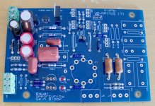
The photo is a picture of my current status. Sockets in R8, R32, and the JFETs. Ready to solder in the DN2540 and confirm the CCS.
Jac
Attachments
Thanks, but you did your point to point or at least on a proto board right? You should see one of my point to point projects. They are more of mess than my desk.
:=)
:=)
Possible Ground Loops?
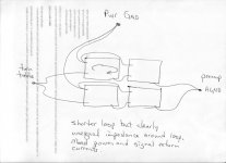
I have been looking at the Didden boards and thinking about ground loops. I am mostly thinking out loud here, but would be grateful your thoughts on the subject.
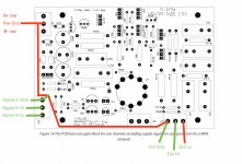
As shown in the first figure, the power, Signal In, and Signal Out grounds have a common connection on these boards. I would guess that they would be a fairly equal potential on the board, given the relatively large ground trace.
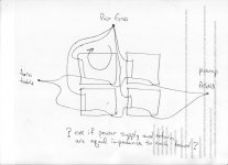
Since we have two boards per channel in series with each other and are using a common B+ and B- power supply ground, running power to each board in parallel would be the natural thing to do. The next figure (sorry for my poor hand drawn illustration) shows the ground wires only. This approach would seem to open the door for multiple ground loops with different impedance. Also, there is no isolation of the power supply currents from the signal circuits. On the other hand, it is nice because it allows the power and return lines to run together and twisted.
The next figure shows a possibility where the second gain stage is powered in kind of a slave to the first gain stage. Power supply and return can remain together and mixed power supply and signal currents are the same as the first option.
The last figure shows using only one power ground per channel (although B+ and B- would still run to the 2nd gain stage board). In this version, both power and signal return would return to the 1st gain stage board through the signal ground connection between the boards. That forces 100% mixing of the power and signal return current. Ground loops still exist, but we have fewer paths for matched impedance.
I honestly don't know which way to go. Input requested.
I suppose I could try more than one and measure output voltage with shorted inputs.
I have been looking at the Didden boards and thinking about ground loops. I am mostly thinking out loud here, but would be grateful your thoughts on the subject.
As shown in the first figure, the power, Signal In, and Signal Out grounds have a common connection on these boards. I would guess that they would be a fairly equal potential on the board, given the relatively large ground trace.
Since we have two boards per channel in series with each other and are using a common B+ and B- power supply ground, running power to each board in parallel would be the natural thing to do. The next figure (sorry for my poor hand drawn illustration) shows the ground wires only. This approach would seem to open the door for multiple ground loops with different impedance. Also, there is no isolation of the power supply currents from the signal circuits. On the other hand, it is nice because it allows the power and return lines to run together and twisted.
The next figure shows a possibility where the second gain stage is powered in kind of a slave to the first gain stage. Power supply and return can remain together and mixed power supply and signal currents are the same as the first option.
The last figure shows using only one power ground per channel (although B+ and B- would still run to the 2nd gain stage board). In this version, both power and signal return would return to the 1st gain stage board through the signal ground connection between the boards. That forces 100% mixing of the power and signal return current. Ground loops still exist, but we have fewer paths for matched impedance.
I honestly don't know which way to go. Input requested.
I suppose I could try more than one and measure output voltage with shorted inputs.
Attachments

between the input signal ground and the output signal ground, what current is anticipated?
might be better to just use separate ground trace for each...
might be better to just use separate ground trace for each...
Remember: balanced. Ground is arbitrary.
Does that mean that any of these approaches is fine?
Jac
The Sign of a Tubie Newbie
I got to the point of putting the tubes in the sockets and powering it up to measure the section balance. So, I have the volt meter clipped to the first of the plate voltage and I turn on the power switch. I glance down and the volt meter is sitting at B+ voltage. Much too high. I look at the LEDs and the tubes and nothing is glowing. Oh NO! I must have done something wrong. Switch off before I burn something up.
After double and triple checking everything, I try again. Still no LEDs. Then, after about 10 seconds, one of LEDs starts to glow. Another 10 seconds and there is a nice orange glow in the top of all of the tubes and LEDs shining brightly. Of course, the plate voltage dropped into the appropriate range.
OK. That's how these things work. They have to warm up first.
Jac
OK. That's how these things work. They have to warm up first.
My biggest laugh of the day!
that WAS pretty funny ...
and brings back good memories.
🙂
mlloyd1
and brings back good memories.
🙂
mlloyd1
My biggest laugh of the day!
Have you ever put your soldering iron on the schematic instead of the circuit?
No, but I can imagine doing that. 🙂
Now, on to more serious issues. I hooked up the amp on the bench to measure DC offset and such. DC is no issue but I have a rather significant difference between the channels. With the input shorted, the output shows 4 mVAC on the right channel and 50 mVAC on the left. The bench meter suggests that this isn't a single frequency. It jumps around with frequencies mostly in the 80 to 100 Hz range. When I hook up a test speaker, the right channel is quiet, but the left has a "whoosh" sound, that is, it sounds like a broad band sound with more strength on lower frequency than Pink noise, for example.
I will try to get an FFT measurement to better understand the noise spectrum.
All the power supplies are as expected and nothing is too hot.
B+ regulated = 122 V on all boards
B- regulated = -15.29 V on all boards
Heater differential voltage = 7.09 VDC on all boards (7 V tubes)
Heater common offset = 26 VDC above ground
CCS all running at 3.9 mA
Section balance 1 V or less
Since the tubes and the JFETs are on sockets, I swapped those out of the left channel to see if I had a bad one. No difference in output.
There doesn't appear to be any AC on the power supplies. 1 mV or less measured close to the tube.
I have the RIAA caps clipped in place so that I can try a couple different choices. As I removed those the output VAC increased to 115 mVAC. That seems to imply that the noise is before the RIAA, but I'm not sure.
I would appreciate any guidance on diagnosing this problem. Thanks in advance.
Jac
Do you have a scope? That sounds like oscillation. I assume all LEDs are lit up?
Also, measure all plate voltages and cathode voltages.
Also, measure all plate voltages and cathode voltages.
- Home
- Source & Line
- Analogue Source
- "Equal Opportunity" MM Pre