I've got a scope but it's old. I'll drag it out and see what I can see.
Yes, the LEDs are all up and the same brightness.
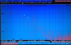
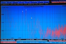
I've attached an FFT of the two channels. I managed to get the right channel in the left picture and vice-a-versa. The trouble is that there is no reference in these measurements since I left the input shorted. It does show about a 5 dB difference in peaks at 305 and 422 Hz, but that might be the result of IMD from an isolation at higher frequencies.
Plate voltage are lower than your 80 V, but I assumed (a mistake I am sure) that the lower voltages might come from my lower CCS current and different tubes. Note, the input tubes are different make than the output tubes. Anyway:
Plate voltage
Input Right Channel - 61.5 V
Input Left Channel - 58.6 V
Output Right - 70.7 V
Output Left - 67.0 V
I will check the cathodes voltage tonite.
One other thought. There is a J1 pin that appears to connect to the tube shield. It doesn't appear to be connected anywhere in the schematics. Am I missing something?
Jac
Yes, the LEDs are all up and the same brightness.
I've attached an FFT of the two channels. I managed to get the right channel in the left picture and vice-a-versa. The trouble is that there is no reference in these measurements since I left the input shorted. It does show about a 5 dB difference in peaks at 305 and 422 Hz, but that might be the result of IMD from an isolation at higher frequencies.
Plate voltage are lower than your 80 V, but I assumed (a mistake I am sure) that the lower voltages might come from my lower CCS current and different tubes. Note, the input tubes are different make than the output tubes. Anyway:
Plate voltage
Input Right Channel - 61.5 V
Input Left Channel - 58.6 V
Output Right - 70.7 V
Output Left - 67.0 V
I will check the cathodes voltage tonite.
One other thought. There is a J1 pin that appears to connect to the tube shield. It doesn't appear to be connected anywhere in the schematics. Am I missing something?
Jac
Attachments
Last edited:
If you have oscillation, it's likely at RF, so yeah, you'll need a scope to confirm. Plate voltages look OK, so no need to measure cathodes.
You know what to do next- swap input boards between channels to see if the problem follows the input or the output boards. Once you've narrowed that down, the next logical step is carefully checking the soldering and all the parts on the duff board (especially resistors, where it's easy to accidentally stick in the wrong value).
Is the J1 pin connected to pin 9 of the tubes? If so, you can either let it float or ground it.
I'll try those things you suggest. Just for the record, the cathode voltage ran between -28 and -83 mV for all 8 sections. No real difference between the two input boards. I also double checked the voltage at the source pin of the JFETs and it is -15.27 VDC.
My oscilloscope is an old Heathkit 10-4550 that my father built years ago. I'm not sure what it's highest frequency is, but the scales run to 0.2 usec/cm, so it should be able to see a couple of MHz at least.
Your guess looks to be correct. With the probe on the high output and the probe ground on the low output, I get noise on the "bad" channel and none on the good channel.
When I sweep from 1 msec/cm to 0.2 usec/cm on the bad channel, I am unable to get to a stable waveform. It looks like random streams across the screen. I took a video with my phone and cut it down to a few seconds showing the bad channel at several scan rates and the good channel. If you are interested to see, PM me with an email address and I'll send you the clip in mpeg or flash, your choice. Anyway, I'm guessing what I am looking at is RF noise or oscillation.
I will work through the steps you suggested and report back. Thanks for your help.
Jac
Diagnosis Update
Found the duff board. Checked all the components on both boards in the duff channel. All resistors correct value and all components soldered properly, although I touched up a couple, just to double check.
I followed the noise as VAC back through the board from the output. Noise is consistent back to the tube. Shorted input, but normal connection between input and output block, here are the AC voltages at the tube pins on the output (duff) block. I also include the pin voltages of the good output block where different for comparison.
Pin 3 and 8 - < 1 mVAC to ground
Pin 2 and 7 - < 1 mVAC to ground
Pin 4 and 5 - < 1 mVAC to ground
Pin 1 and 6 - 55 to 58 mVAC to ground, 110 - 115 mVAC across 1 to 6 (duff)
Good output block pins 2-5, 7, and 8 all < 1 mVAC
Good output block pins 1 and 6 - 1 to 2 mVAC, ~ 4 mVAC across 1 to 6 (good)
I can trace the 110 mVAC up through the CCS, but the output of the B+ voltage regulator is 121 to 122 VDC and essentially zero VAC. Is it possible for the CCS to oscillate? How would I chase this?
Thanks in advance.
Jac
Additional Info
It appears to be an interaction between the first and second gain blocks. I disconnected the signal connection between the blocks and shorted the input of the output block which had been the duff block. With the two blocks disconnected, the noise was gone and the output read 4 mVAC. I reconnected the two blocks and the noise reappeared.
The noise doesn't appear to care if the input block gain is shorted or open circuit. Noise stays the same.
I connected the output block to the input block by the signal ground wire only (signal high and low remain open circuit) and the noise remained gone.
I am wondering if there is an interaction between the power supply wires and the boards. I am currently wired with power and ground to all boards in parallel.
Jac
I can trace the 110 mVAC up through the CCS, but the output of the B+ voltage regulator is 121 to 122 VDC and essentially zero VAC. Is it possible for the CCS to oscillate? How would I chase this?
Yes, it's possible for a CCS to oscillate- I haven't had it happen yet, but with high frequency devices, it's always lurking. Do you see AC at both plates on the duff board or just one plate? Did you check the B- supply to the FETs? Are their gates tied to ground through the input resistors?
Yes, it's possible for a CCS to oscillate- I haven't had it happen yet, but with high frequency devices, it's always lurking. Do you see AC at both plates on the duff board or just one plate? Did you check the B- supply to the FETs? Are their gates tied to ground through the input resistors?
Yes, there is AC at both plates at equal level and apparently out of phase because the AC voltage across the 2 plates is twice that of a single plate to ground.
B- supply to the FETs is -15.27 VDC with no AC. There is a 0.47 uF cap from B- to ground just before the FETs.
Per your article schematic, the output board has 100 Ohm resistors in series with the FET gates and is not referenced to ground on the board, but is referenced to ground by the 1 MOhm resistors on the output of the previous board. Of course, it would be easy to add a ground reference because the location for R1 and R2 (input impedance on the input board) have been left open.
I continue to wonder about the interaction between the boards. When I initially swapped the input boards to find the duff board, the noise went with the input board and was present on the input board. Then the input board became quiet, but the output board became noisy. The output board has remained noisy since then.
The fact that I can make the noise come and go by connecting and disconnecting the signal connection between the boards has me curious.
Jac
After your question about input ground reference resistors, I put a couple 10k resistors referenced to ground in the input terminal block. This cut the AC across the plates from 110 to 40 mV.
Jac
Jac
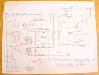
OK, could you sketch out a detailed pic of your grounding scheme (including any connections to the chassis)? And double check it against the actual unit, not what you intended it to be.
edit: One more thing- what is the idss of your FETs?
edit: One more thing- what is the idss of your FETs?
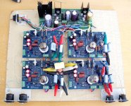
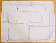
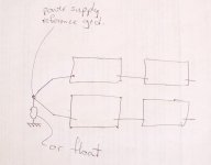
At present, the raw power supply is in an enclosure with safety ground as shown in the sketch, but the heater regs, final power filters for B+ an B-, and the 4 gain blocks are on a plywood board. See the first photo. The power supply board (heater regs, etc) is at the top with the gain blocks below. Note, I am planning on trying a couple of different RIAA and output caps, so those connections are currently clipped to faston tabs. I removed the RIAA caps on the upper (noisy) channel to see if they affected the noise.
The 2nd and 3rd photos are sketches of the power layout including ground scheme. For the 3rd photo, I have only shown the grounds. The B+ and B- power run from the power supply board at the top to the gain boards parallel to the grounds and twisted together.
The heater plus and minus have an offset common (per His Master's Noise Heater supply) which is on the power supply board. Only the H+ and H- wires run to the boards, no parallel ground.
FET Idss
Input boards
upper - 5.0, 6.2 mA (note, I have tweaked FET pairs to get good section balance)
lower - 6.2, 4.8
Output boards
upper - 5.5, 4.4
lower - 6.3, 5.8
My original FET matches were all less than 0.1 mA with my best pairs within 0.01 mA. Gains were well matched as well. Is it possible that my swapping FETs to better balance the sections is a potential cause for the noise?
By the way, these FETs are Toshiba 2SJ74, not Linear LSJ74. I have traced Id versus Vgs for several of the transistors and they follow the data sheet, so I believe they are real.
Thanks again for helping me to try to figure out this noise. I confess, I hooked it up in my main system and it sounds amazing, even with the noise. I am very motivated.
Jac
Attachments
Look at your grounding sketch- you have a few loops in it, which you very much would want to avoid.
The idss question was because of gate current- if the idss is too low (i.e., near the 4mA operating current), you'll have gate current, which will not be a good thing. See if you can find some FETs in your collection with idss of 6mA or higher, just to be safe. Or reduce the current to 3mA, which is still on the low-noise sweet spot.
The idss question was because of gate current- if the idss is too low (i.e., near the 4mA operating current), you'll have gate current, which will not be a good thing. See if you can find some FETs in your collection with idss of 6mA or higher, just to be safe. Or reduce the current to 3mA, which is still on the low-noise sweet spot.
SY,
In an earlier post (#157), you suggested that section balance of 10 V or less would be OK, although lower is obviously better. Of course, you have very well balanced tubes and got 0.5 V section balance per the article.
I can easily get my Idss between 5.6 and 6.3 and have better Idss matching. That sounds like a good thing to do. Essentially, that is how I built it originally before I started tweaking section balance. With the higher Idss, I expect to get section balance in the 2 to 5 V range. Am I correct that I will loose a touch of CMR, but otherwise should be OK?
I also think I am going to add an input ground reference. Do you have any input on the resistor value for an input ground reference? I was thinking about 10k or 22k, depending on what I can find in the parts drawer.
The reason for adding the ground reference is that adding 10k resistor ground reference brought the noise down to 35 - 40 mVAC range. Today I removed the RIAA caps on the other channel and was interested to find that the output went from 4 mVAC to 35 - 40 mVAC.
As for the ground loops, I have been aware of this as a potential issue and have done experiments on different configurations. None of them changes the noise, however. Even though it doesn't affect the noise, I will go forward with the last picture in post 170.
Finally, I will see what I can do about dropping the CCS to about 3 mA. Currently it is at 3.9 mA.
Thanks again for your help.
Jac
You may not lose any CMR at all. It's really more dependent on matching of mu than anything else, and that's a variable which is pretty consistent.
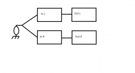
In my build, nothing is grounded directly to the chassis. The signal ground is connected at one point (the junction of the input resistors) to the chassis through a groundbreaker (100R with a parallel 0u01 cap and two 69'ed diodes, which I symbolized as an oval in my sketch). No loops- the grounds of the two channels only meet at that input point.
In my build, nothing is grounded directly to the chassis. The signal ground is connected at one point (the junction of the input resistors) to the chassis through a groundbreaker (100R with a parallel 0u01 cap and two 69'ed diodes, which I symbolized as an oval in my sketch). No loops- the grounds of the two channels only meet at that input point.
Attachments
Is your power ground completely separate from your signal ground? Or in some way isolated from signal ground? The way these boards are designed, power and signal ground are on a single PCB trace. Since the power ground is common to both channels, loops are possible between channels. Maybe something that should be considered before additional boards are made.
Jac
Jac
As long as the two channels' grounds only connect together at one point, there's no loop. Remember, in a balanced circuit, "ground" is notional as far as signal goes- amplification is differential.
Noise Update
1. Revised ground scheme to last sketch.
2. Installed FETs with high Idss. Noisy channel Idss now 6.16 to 6.3 mA. Section balance isn't too bad. From 0.37 up to 3.0 V.
3. Added ground reference resistors to the input of the Output Gain Block (22k).
Results
High frequency noise is gone.
Audio frequency noise has dropped from 110 - 115 mVAC to about 17 mVAC. Sounds much quieter too. At this level, it's not ideal, but you can listen to music.
It looks like raising the Idss helped. I will order resistors to lower the CCS current. I didn't have enough of appropriate values to try it. You said that 3 mA would be OK. What's the "bottom of the sweet spot"? Is 2.5 mA too low?
It is odd that I still have noise in only one channel. I may have a noisy component, although I don't know why it would be on both sections if it was one component. I may try swapping out CCS mosfets and resistors to see if anything changes.
Thanks again for your help.
Jac
The current isn't super critical- Merlin's data on tube noise showed a rather shallow minimum for the ECC88.
Also, remember that noise in one section will be amplified since it will be differential mode.
I'm delighted that you're making progress! I only learn stuff when something goes wrong.
Also, remember that noise in one section will be amplified since it will be differential mode.
I'm delighted that you're making progress! I only learn stuff when something goes wrong.
It's gotten a little quiet around here. I bought the last set of boards from JP and Jim's Audio is selling matched jfets(while supplies last). A little pricey but hey, the supply is thin for Tosh jfets.
It will be a slow build as time and finances permit, but I intend on grabbing the hard to get stuff first.
BTW SY, absolutely gorgeous day today! Bluebonnets have been in fine form.
It will be a slow build as time and finances permit, but I intend on grabbing the hard to get stuff first.
BTW SY, absolutely gorgeous day today! Bluebonnets have been in fine form.
Yeah, I'm backlogged and low on sleep. And the ADHD is kicking in. For example I noted a distinct topological resemblance between the EO board and some of the Gilmore Stax headphone drivers. My Koss ESPs are off for repair.. I have some spare EO boards.
- Home
- Source & Line
- Analogue Source
- "Equal Opportunity" MM Pre