It’s a Shapeoko 4. It’s been a lot of fun learning to use it and now I can’t live without it. Poor woodworker that I am.
Ummmmmm....with the shown EL34 grid circuit resistance, not much of A2 is going to happen.
A triode on the bottom and 'FET on top has made for some fine signal amplifiers IME. Have even built a triode on the bottom and pentode on top as a composite load circuit( lots of B+ required, and not much signal voltage.
Douglas
A triode on the bottom and 'FET on top has made for some fine signal amplifiers IME. Have even built a triode on the bottom and pentode on top as a composite load circuit( lots of B+ required, and not much signal voltage.
Douglas
The el34 G1 circuit Z is very low. It’s connected to a fixed 25v.
Have a closer look at the 25v supply

Have a closer look at the 25v supply

I'd ask the question; what is it for? so to say, what benefit are you looking to derive?
Douglas
Douglas
Generally speaking my goal is always the same, my own entertainment. This is ostensibly what I do for fun. If I find I’m not enjoying the process I’m doing something wrong. More specifically I get no enjoyment out of building other people’s designs or building typical topologies. So that may explain some of my design choices perhaps.
For this exact project it resulted from a conversation with my friend Leandro who is much smarter than I am but somewhat new to electronics. As a result he asks extremely good questions that us more experienced designers would never think of. So this amp is the answer to that question. The answer being “yes”.
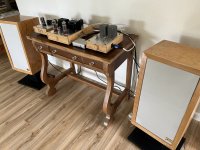
More practically speaking this amp will be used to power my medium efficiency speakers in my stereo system. For example here is a photo of the amp driving my grandfather’s AR3a.
For this exact project it resulted from a conversation with my friend Leandro who is much smarter than I am but somewhat new to electronics. As a result he asks extremely good questions that us more experienced designers would never think of. So this amp is the answer to that question. The answer being “yes”.
More practically speaking this amp will be used to power my medium efficiency speakers in my stereo system. For example here is a photo of the amp driving my grandfather’s AR3a.
Attachments
The el34 G1 circuit Z is very low. It’s connected to a fixed 25v.
Also, what is the resistance reading at the wiper of your VR101 bias adj? It seems that 90% of your driver signal is lost before it gets to the EL34. Are you getting part/most of your output power from driving the MOSFET?
There is no signal present at G1. All of the signal is present at the mosfet gate. The mosfet may be thought of as a modulated current source. The output stage is a Cascode. This is typically found in signal amplification stages but in this case it’s the output stage.
''...There is no signal present at G1. All of the signal is present at the mosfet gate. The mosfet may be thought of as a modulated current source. The output stage is a Cascode. This is typically found in signal amplification stages but in this case it’s the output stage...''
Yes, OK, I'm tracking along now, finally. Is the EL34 there simply for Z matching to a conventianal OPT? Here's what I see. The EL34 K is 44v and 25v on G1 for a bias of -19V. Plate would be @310v for the operating point, and .088mA of throughput for 27.5W Pdiss. The book says @6W of plate signal power. Since the MOSFET is a serial device to the EL34 it passes the same current. What is the role of the MOSFET if the EL34 is already running at 100% of Pdiss and can't be pushed for more swing along the loadline into A2 even if an EL34 was built to take any grid current? Are you puting more than 19v peak signal on the K out of the MOSFET? How far below 25v on the K are you going to get the 10W to the speakers? Or is that 4W of extra A2 signal power? These are all just paper numbers so I'm curious if they're in the ballpark. It seems from the title of the thread and the silkscreening on your PCBoard that A2 operation is a major part of the design goals. Applaud for the design work. Can't imagine the time involved for this build. We all do this stuff for our own pleasure, for sure.
Yes, OK, I'm tracking along now, finally. Is the EL34 there simply for Z matching to a conventianal OPT? Here's what I see. The EL34 K is 44v and 25v on G1 for a bias of -19V. Plate would be @310v for the operating point, and .088mA of throughput for 27.5W Pdiss. The book says @6W of plate signal power. Since the MOSFET is a serial device to the EL34 it passes the same current. What is the role of the MOSFET if the EL34 is already running at 100% of Pdiss and can't be pushed for more swing along the loadline into A2 even if an EL34 was built to take any grid current? Are you puting more than 19v peak signal on the K out of the MOSFET? How far below 25v on the K are you going to get the 10W to the speakers? Or is that 4W of extra A2 signal power? These are all just paper numbers so I'm curious if they're in the ballpark. It seems from the title of the thread and the silkscreening on your PCBoard that A2 operation is a major part of the design goals. Applaud for the design work. Can't imagine the time involved for this build. We all do this stuff for our own pleasure, for sure.
You’re in the ballpark definitely. In this configuration the MOSFET is a gain stage. Small changes in the gate voltage result in large changes in the Drain. The first 3.5-4w are within the typical range you mentioned. The difference between the 25v grid and the 44v cathode. So 19v x2 peak to peak. That’s what the el34 cathode and MOSFET drain are swinging in terms of voltage. After that the cathode/drain begins to swing below G1. Now it should become clear why G1 is held at +25v. So the difference between the 3.5w or so and 10w is the A2 operation. I actually have current sensing LEDs visible at the top plate that show exactly when current begins to flow in the G1 circuit. It’s fun to see them flash a bit when the amp is pushed hard.
The tube is being run at max dissipation and the hotter the bias the more power it makes to a certain point. Some of the power supplied to the output transformer is coming from the MOSFET. The power ratio is the same as the idle dissipation ratio between the tube and the MOSFET.
One of the benefits of this configuration is A2 is achievable with no negative supply rail.
''...So 19v x2 peak to peak. That’s what the el34 cathode and MOSFET drain are swinging in terms of voltage...''
''...The first 3.5-4w are within the typical range you mentioned. ...''
This is your A1 at the speaker taps, yes? 19v of drive gets you 4W there? That seems right. I have a 6L6 SE with 310v plate and -21 and get just about that, too.
I believe that is all within the A1 portion of the loadline. Until you put more than -19v signal on the K's 44v it's still above 25v G1 so no grid current yet. If the K goes to 24v, then A2 power is flowing. What does your scope tell you for peak K signal when the LEDs start flickering? And then at 10W ... What do the LED's actually measure? They seem very isolated from the grid of the EL34 at the supply input to 25v regulator?
I haven’t actually scoped the exact point where G1 starts flowing in relation to the cathode swing. But it’s really obvious when A2 begins in practice. The the entire character of the amp changes. The distortion spectrum and grid current are easy to see. If you have a look at the measurements, particularly the distortion sweeps you can see A1 distortion and A2.
Also I should mention that the only thing stopping the FET from pulling the cathode all the way to GND is the RDSon and the 51R source resistance. So it can swing quite low. I carefully adjusted the G1 voltage up until the amp didn’t make any extra power. Meaning driving the cathode more and more negative results in diminished returns. The tube can only be so “ON” so to speak.
Wonderful process, Young! 
Quote:
"here is a photo of the amp driving my grandfather’s AR3a."
How does this amplifier feed these large diet speakers AR3a? However, the shape of your AR is very good. Was this pair refinished?
BTW, BUG is your Symbol. Isn't it? Is there a chance that PCB or kit offerings follow?
Joe
Quote:
"here is a photo of the amp driving my grandfather’s AR3a."
How does this amplifier feed these large diet speakers AR3a? However, the shape of your AR is very good. Was this pair refinished?
BTW, BUG is your Symbol. Isn't it? Is there a chance that PCB or kit offerings follow?
Joe
The AR3a are just fine in a medium size room at sane levels with 10w. I have restored these and they’re operating perfectly now.
I’m still thinking if I want to provide PCBs. There are pros and cons. I’ve of course already made the circuit public so anyone can build the amp already if they so choose.
I’m still thinking if I want to provide PCBs. There are pros and cons. I’ve of course already made the circuit public so anyone can build the amp already if they so choose.
Nice design, but I wonder what happens when the grid current starts flowing? The way I see it there must be a negative step in the plate current when the grid goes positive, as the output stage is controlled by a modulated CCS?
One possible solution would be to connect the drain of the mosfet that feeds the grid to the plate, that would ensure that the current through the output transformer is exactly equal to the cathode current, grid current or not.
One possible solution would be to connect the drain of the mosfet that feeds the grid to the plate, that would ensure that the current through the output transformer is exactly equal to the cathode current, grid current or not.
Thanks Fuling. Your comment really made me think. I do think that ideally you’re right, the best case scenario would be to somehow send the electrons emitted by the grid through the output transformer primary. It would probably boost power fractionally. Though the idea that the FET on the cathode is limiting current is probably not an issue. By the time the stage is clipping on the negative plate swing FET is very “on” and the feedback loop from the output transformer secondary is also trying to linearize by turning the FET even more “on”, so to speak. But I do agree that another 15ma of current through the output transformer isn’t nothing.
I don’t think the grid supply FET would survive being fed directly from the plate though. Depending on load Z the swing there can be unpredictably large. I’ll. Think about it.
I don’t think the grid supply FET would survive being fed directly from the plate though. Depending on load Z the swing there can be unpredictably large. I’ll. Think about it.
I think it’s a lot like a pentode output stage. We’d really prefer the screen current go through the output transformer, but it’s hard to have the screen voltage be regulated and travel through the output transformer.
Yes, it would take one heck of a mosfet to survive the full plate swing. On the other hand, it would only pass current while the voltage across it is close to the lowest point. Perhaps one of those new IXYS 1700V parts would make it?
The voltage feedback from the output to the CCS probably takes care of most of the issues here and since this amp only reaches class A2 during peaks, it's probably not a real problem. I've been thinking about using the same topology to drive high mu transmitter triodes into class A2 but the grid current might become a bigger problem there as it flows for most part of the cycle.
The voltage feedback from the output to the CCS probably takes care of most of the issues here and since this amp only reaches class A2 during peaks, it's probably not a real problem. I've been thinking about using the same topology to drive high mu transmitter triodes into class A2 but the grid current might become a bigger problem there as it flows for most part of the cycle.
- Home
- Amplifiers
- Tubes / Valves
- EL34 A2 Cascode SE triode