Thanks Elvee!!The operating principle is now different, therefore the sensor transistor is now Q2, and the bias pot could be R18 for example
So the upper output device's gate has fixed bias voltage now, and only lower device's (M2) gate voltage will be affected
by Q2, right?
Last edited:
Both will be affected: Q2 controls the common mode current, which sets the quiescent current, and the audio signal is converted into differential drive to the MOSFets by the IRF510 LTP.
This amplifier is a beginner's project, and to apply these measures without too many risks requires minimal competences to achieve a good thermal contact between the transistors and the heatsink.
An amateurish attachment might be enough to sustain the permanent 5 ~ 7W caused by the quiescent current, but as soon as a "thermal event" caused by the program contents and the load occurs, it will drive the amp into a fast and irrecoverable thermal runaway.
With reasonably sized resistors, this risk is mitigated.
First off, thanks for posting this easily digestible project!
I had heard ( perhaps incorrectly ) that amplifiers with mosfet output stages were immune to thermal runaway, can you elaborate on this?
To summarize: two very different breeds of FETs exist, lateral and vertical.
Vertical ones behave very much like BJTs up to high currents. The Vto is larger in absolute value than the Vbe, but it follows broadly the same kind variation law according to temperature.
Lateral ones display the opposite behavior, and do not risk thermal runaway or require balancing resistors when paralleled.
They are also rarer, more expensive and much less efficient.
You can easily find more detailed information on this forum or on the net if you use the correct search terms
It could look like this (not for construction, just a concept):
Another possibility is a CircloMos converted to a single supply (easily done):
https://www.diyaudio.com/forums/solid-state/154388-cheap-dirty-circlomos.html?highlight=circlomos
Very interesting. I'm not sure I understand everything you did, but it works a lot better than I might expect. This is an example of the things I've been doing with it.
Attachments
The idea of using the tail MOS as a Vgs-multiplier to set the quiescent current is smart, and looks advantageous because it allows the elimination of the G-S resistors, thus increasing the loop gain, but it is not without problems: the voltage sensed will be "polluted" by the class B current through the MOS and its source resistor, and this arrangement requires a specific hierarchy of Vto's.
However, despite the higher gain it does not deliver.... the THD is in fact higher.
Why this paradox?
The original circuit was designed for ~square-law operation, and this is now lost, and the increase in loop gain does not compensate for loss of linearity
However, despite the higher gain it does not deliver.... the THD is in fact higher.
Why this paradox?
The original circuit was designed for ~square-law operation, and this is now lost, and the increase in loop gain does not compensate for loss of linearity
It looks like a very good idea, and it is applicable to other versions too.
It is one of the reasons why I said the N version is a concept: it lacks that kind of refinement and streamlining before it becomes an actually buildable project.
The sim examples could probably be made to work in reality, but a good DIY project should be reasonably resilient and effective at coping with "contrasted" contexts
Another issue that needs to be tackled with the N version, if it is to become actually buildable, is the quiescent current stability vs. temperature and vs. supply voltage.
Currently, none of the variants (Steveu's and mine) is acceptable in those respects: ideally, Iq should be reasonably stable for supply variations of, say +/-25% at least, and the overall tempco in sim should be negative, but reasonably so (the tempco needs to be negative, because in the real world, the thermal contact between the sensor and OP transistors is largely imperfect)
Currently, none of the variants (Steveu's and mine) is acceptable in those respects: ideally, Iq should be reasonably stable for supply variations of, say +/-25% at least, and the overall tempco in sim should be negative, but reasonably so (the tempco needs to be negative, because in the real world, the thermal contact between the sensor and OP transistors is largely imperfect)
and next issue
So this addresses those issues somewhat.
1. a diff-amp input does not drop a lot of bias on the feedback so the output remains centered over a wide range of supply voltage. An LTP current source would be better but I'm trying to keep this as simple as possible, so I picked R20 to provide enough current from 50VDC.
2. Adding a ~Darlington transistor to M7 makes it more stable over a range of currents that come from different supply voltages. It also adds the BJT thermal behavior to the vto multiplier. Enough?
And the THD is down again. And I'm ~happy with the clipping behavior when you reduce the supply to 50V. Complicated circuits tend to do strange things when over-driven.
Adding current sources would solve the variable supply issues but then you have a ~complicated circuit. I really like current mirrors between the diff-amp and the VAS, but again, that's more transistors.
An issue I would like to hear from LV about is the trade-off between VAS current and FET slew. I don't like large resistors. Just how fast do we need to slew? Class-B drivers would reduce the resistor heat but boot strapping drivers gets messy.
Another issue that needs to be tackled with the N version, if it is to become actually buildable, is the quiescent current stability vs. temperature and vs. supply voltage.
Currently, none of the variants (Steveu's and mine) is acceptable in those respects: ideally, Iq should be reasonably stable for supply variations of, say +/-25% at least, and the overall tempco in sim should be negative, but reasonably so (the tempco needs to be negative, because in the real world, the thermal contact between the sensor and OP transistors is largely imperfect)
So this addresses those issues somewhat.
1. a diff-amp input does not drop a lot of bias on the feedback so the output remains centered over a wide range of supply voltage. An LTP current source would be better but I'm trying to keep this as simple as possible, so I picked R20 to provide enough current from 50VDC.
2. Adding a ~Darlington transistor to M7 makes it more stable over a range of currents that come from different supply voltages. It also adds the BJT thermal behavior to the vto multiplier. Enough?
And the THD is down again. And I'm ~happy with the clipping behavior when you reduce the supply to 50V. Complicated circuits tend to do strange things when over-driven.
Adding current sources would solve the variable supply issues but then you have a ~complicated circuit. I really like current mirrors between the diff-amp and the VAS, but again, that's more transistors.
An issue I would like to hear from LV about is the trade-off between VAS current and FET slew. I don't like large resistors. Just how fast do we need to slew? Class-B drivers would reduce the resistor heat but boot strapping drivers gets messy.
Attachments
The DC centering is not a problem, even without diff: the drop on the FB resistor is highly predictable because the current is defined by R10 and the reference input of the VAS.1. a diff-amp input does not drop a lot of bias on the feedback so the output remains centered over a wide range of supply voltage. An LTP current source would be better but I'm trying to keep this as simple as possible, so I picked R20 to provide enough current from 50VDC.
This means that a zener or a LED(s) in series with the input bias resistor is sufficient for a good compensation.
Regarding supply variation, it is not perfect, but it is good enough (I increased R9 to get a more realistic Iq):2. Adding a ~Darlington transistor to M7 makes it more stable over a range of currents that come from different supply voltages. It also adds the BJT thermal behavior to the vto multiplier. Enough?
The tempco is now negative, but it is much too strong: for a 10 to 80° range, it varies in a 10 to 1 ratio, which is excessive (1 to 1.5 or 2 would be more reasonable)
The complexity is already far beyond the initial scope of the project, but you are of course free to propose/test any circuit.And the THD is down again. And I'm ~happy with the clipping behavior when you reduce the supply to 50V. Complicated circuits tend to do strange things when over-driven.
Adding current sources would solve the variable supply issues but then you have a ~complicated circuit. I really like current mirrors between the diff-amp and the VAS, but again, that's more transistors.
For my part, I will try to keep all the versions, including the N one as minimalist as possible
An issue I would like to hear from LV about is the trade-off between VAS current and FET slew. I don't like large resistors. Just how fast do we need to slew? Class-B drivers would reduce the resistor heat but boot strapping drivers gets messy.
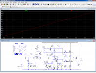
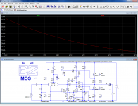
The main problem currently is caused by the VAS Miller: the positive SR is 8.6V/µs and the negative one 25V/µs, clearly insufficient.
A cascode improves matters for the positive, 80V/µs, but the negative slew has a nasty artifact, probably caused by M2 M6's Miller:
Attachments

In my day we designed stuff on paper then vero-boarded it.
LTSPICE makes the job less prone to problems.
And the good old Chinese supply pcb's for peanuts once you get it working well.
LTSPICE makes the job less prone to problems.
And the good old Chinese supply pcb's for peanuts once you get it working well.
tempco and slew
I ran into some strange behavior, including trying the cascode transistor, but I wanted to share a better tempco alternative, ie use a PNP at Q2. The tempco is still negative but not as much because the BJT is not part of the multiplier.
How much slew is enough is an old argument, and you could argue that 2 pi 20k Vp or 0.126/uS * VPk (6.3V/uS for 50VPk) is enough. But I think at least 2 to one margin is wise, ie 12V/uS. Of course if you want a 100KHz power bandwidth then you want more.
I am more concerned with the high power resistors and VAS transistor, so I have reduced the heat in this version.
Hopefully I will figure out what is causing some odds things and make the cascode etc work better. I did get some very low distortion at 1KHz but then I had bad things at 20KHz. I am ignoring my own advise to not waste time on this but hey, I'm retired and I enjoy it.
Cheers,
Steve
Attachments
Last edited:
I want a slew rate so high that the error signal (Vin - Vfeedback) when producing a max amplitude 44 kHz sine wave, is only 10% larger than the error signal when producing a max amplitude 440 Hz sine wave.
I realize the way I biased the lower FETs creates a huge inrush at startup, and it just gets worse when you look at lower frequencies. Spice hides this unless you specify no cap pre-charge. Maybe there is some clever start-up circuit that can pre-charge the filter but DC regulation is at odds with AC filtering.
But I learned a couple things from LV and this was a completely different approach to quasi-comp output. Reminds me of some other lessons that take a bit of a voyage to sink in. There is more to amplifiers than frequency response, distortion and efficiency.
But I learned a couple things from LV and this was a completely different approach to quasi-comp output. Reminds me of some other lessons that take a bit of a voyage to sink in. There is more to amplifiers than frequency response, distortion and efficiency.
Elvee,
For the N version you published several posts ago -
As for LEDs here - each LED is supposed to drop approx 5V, correct?
For the N version you published several posts ago -
As for LEDs here - each LED is supposed to drop approx 5V, correct?
Last edited:
Elvee,
For the N version you published several posts ago -
As for LEDs here - each LED is supposed to drop approx 5V, correct?
See:
https://www.mouser.com/datasheet/2/308/qtlp690creoyag-1195966.pdf
The typical forward voltage spec is 2.0, 2.4 V max, and that is at 20mA. We are only using 2.6mA so it's going to be less than that. Simulation shows 1.8V each. ~2V is standard forward drop for colored LEDs.
You never use the reverse voltage of LEDs, except if there is any danger of reverse bias and then you might have to protect them with another diode.
Last edited:
Thanks Steve.
See:
https://www.mouser.com/datasheet/2/308/qtlp690creoyag-1195966.pdf
The typical forward voltage spec is 2.0, 2.4 V max, and that is at 20mA. We are only using 2.6mA so it's going to be less than that. Simulation shows 1.8V each. ~2V is standard forward drop for colored LEDs.
You never use the reverse voltage of LEDs, except if there is any danger of reverse bias and then you might have to protect them with another diode.
As Steveu said;Elvee,
For the N version you published several posts ago -
As for LEDs here - each LED is supposed to drop approx 5V, correct?
A gentle reminder: the N-version is a totally speculative exercise, and only exists in virtual form inside the memory of a few computers. Not a single splash of solder has been spent on it, unless someone has been foolish enough to try it (will you be that person?)
A gentle reminder: the N-version is a totally speculative exercise, and only exists in virtual form inside the memory of a few computers. Not a single splash of solder has been spent on it, unless someone has been foolish enough to try it (will you be that person?)
I know 🙂
As soon as I'm done with Circlophone build (very soon), this will be the next project. For some strange (historical ?) reason, I'm only interested in Quasi amps..
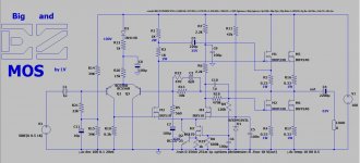
- Home
- Amplifiers
- Solid State
- Easy-MOS is a simplistic, efficient and evolutive all-MOS amplifier for beginners