I think this AC measurement better done with an oscilloscope.
I did some testing with other amps DIY amps but also very highly respected commercial amps and they all had some ACV on the output.As I said it earlier with the input shorted it drops from 4mV to 2.1mV for me thats ok.Get back to it when the other channel is build like I intend to do.
.As I said it earlier with the input shorted it drops from 4mV to 2.1mV for me thats ok.
.
With input shorted, an good amp shouldn t produce more
than 50uV (0.05mV) of output AC residuals...
With input shorted, an good amp shouldn t produce more
than 50uV (0.05mV) of output AC residuals...
It drops to 0.001VAC when shorted not shorted it's 0.004
Hi Meanman
Yes, exactly. Thank you!
Now we are talking of 2 mV, not 4 mV. That is 6 dB better at about 83 dB below full output. Measurements of amps with open inputs include induced noise which you have verified as higher than amp noise itself. It's irrelevant to the problem so we only read output with shorted input. That "Fluke" adds credibility. My bench model reads 1.35 mV. A mid-range Hand-held reads 0.001VAC.
Obviously, There is a practical limit to how precisely you can quote readings with flex wired probes. They are receivers of EMI from all sources around, open or shorted. Even a heater I use here increases readings. The PC sends it into orbit! Nonetheless, You have a reading of 0.0021 when the initial shorted reading is 0.001VAC, according to to your figures. I assume that the range has changed to allow another digit resolution here. Well, realistically, only a figure of 1 mV can be considered the likely Hum figure.
Thats around 88 dB below full ouput into 8 ohms.
The fact that you say it is hum and you can no longer hear it with your ear right in the speaker (thats where I have to listen) says: "mission accomplished" regardless of what meters at the extremes of their imprecision say! I would personally try to get this lower by rearranging and tidying power leads to and near the amplifier input. Best arrangement IMHO is to twist both rail supplies tightly together and lead in from below the power end, split to the fuse spades. It's basic; read the meter and adjust for lowest reading if possible and with safety! Remember, under load, power leads will radiate hum and noise straight into sensitive input and feedback circuits. This is a known source of distortion, and turns brilliant sound into ordinary. It's difficult without expensive gear to tackle that problem under load, however......For the time being, Just Enjoy!
I've to take back my words about the bass is shy installed a 10µF MKP for C1 and tested again holy cow suddenly there was a huge bass sound I liked very much.Carlos thank you for this amp very good sonics not bass shy at all.
Did some testing with using other values for C1.Starting with 10µF strong bass,4,7µF strong bass,1,5µF strong bass and 0,47µF strong bass.My conclusion why using 10µf when 0,47µF is enough?Now test what diffirent values do with the hights.
C1 forms a filter, according to the amp's input impedance. The higher the value, the lowest the bass cut frequency is. 10uF is a nice value, don't change it.
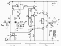
R2 & C1 form the high pass filter.
10uF and 10k give an RC of 100ms. This is equivalent to an F-3dB =1.6Hz and F-1dB ~3Hz.
The NFB cap is just a little small compared to this.
I recommend that NFB cap >= sqrt(2) * C1 * R2 / R7
If you keep 10uF for R1 then C7>=300uF.
or alternatively keep R7=470r and C7=220uF and change C1<=7uF
I would be tempted as a first experiment to add 100uF to C7 to hear if there is any discernable difference.
R2 & C1 form the high pass filter.
10uF and 10k give an RC of 100ms. This is equivalent to an F-3dB =1.6Hz and F-1dB ~3Hz.
The NFB cap is just a little small compared to this.
I recommend that NFB cap >= sqrt(2) * C1 * R2 / R7
If you keep 10uF for R1 then C7>=300uF.
or alternatively keep R7=470r and C7=220uF and change C1<=7uF
I would be tempted as a first experiment to add 100uF to C7 to hear if there is any discernable difference.
What benefit do we've with this?
the input filter defines one end of the bandwidth of the amplifier. It attenuates signals that might otherwise interfere with correct operation. The low pass filter defines the other end of the bandwidth. Both are necessary and both are passive.
The NFB cap is crucial to sound quality and should never have a significant DC nor AC voltage across it.
If the NFB cap is too small it will see some AC voltage and will contribute to amplifier distortion. The lower the voltages on the NFB cap, the better the amplifier should sound.
The DC voltage across the NFB cap when operating correctly is ~=DC voltage across R2 (about 20mVdc to 100mVdc)
I think the bootstrap cap (C10) is also a bit small but others have said it is OK at 47uF.
I am staggered that you can't hear a difference between 10uF and 470nF as C1. 470nF (4.7ms) gives F-1dB ~60Hz.
Last edited:
This is also the difference in design between Dx Blame ST and Blameless.
meanman, you can wait till the designer is back and discuss C7 with him, it is much better to wait for his answer. IMO, you are supposed to leave the design as is as you agreed to build Dx Blame ST, this will confuse other builders as well.
Conclusion: The amplifier was designed this way. No need to start calculations all over again, book calculations I mean, wait for the designer to hear from him why he decided on that value this way.
Attachments

Last edited:
I'm in no need to change the value of C1 and C7 it's ok for me.I do hear a little difference in bass sound when I use 0,47µF but not much.
This is also the difference in design between Dx Blame ST and Blameless.
meanman, you can wait till the designer is back and discuss C7 with him, it is much better to wait for his answer. IMO, you are supposed to leave the design as is as you agreed to build Dx Blame ST, this will confuse other builders as well.
Conclusion: The amplifier was designed this way. No need to start calculations all over again, book calculations I mean, wait for the designer to hear from him why he decided on that value this way.
The way the CCS are implemented is very bad...
This is also the difference in design between Dx Blame ST and Blameless.
meanman, you can wait till the designer is back and discuss C7 with him, it is much better to wait for his answer. IMO, you are supposed to leave the design as is as you agreed to build Dx Blame ST, this will confuse other builders as well.
Conclusion: The amplifier was designed this way. No need to start calculations all over again, book calculations I mean, wait for the designer to hear from him why he decided on that value this way.
Metal,
I give you the certainty that I don't change anything of the design.After my amp is completed we can tweak it together with Carlos to make it even better.
Hi Meanman, what were you using at C1 before you put the 10 uF MKT in and got a huge improvement in Bass? BTW, do you know the approximate bass response of your speaker? i.e.-3dB response point.
Wahab, you realise the designs posted by Metal are not DX Blame ST or ES. They are the Blameless model design by D.Self. The differences are only indicated. Anyway, you have seen the actual design before. It has Bootstrap VAS and a simpler diode reference for the LTP CCS. The input circuit is also different as shown. The Schematic is at the beginning of the thread and via a link to Greg Erskine's website. There are just a number of small capacitor differences between ST and ES.
Wahab, you realise the designs posted by Metal are not DX Blame ST or ES. They are the Blameless model design by D.Self. The differences are only indicated. Anyway, you have seen the actual design before. It has Bootstrap VAS and a simpler diode reference for the LTP CCS. The input circuit is also different as shown. The Schematic is at the beginning of the thread and via a link to Greg Erskine's website. There are just a number of small capacitor differences between ST and ES.
Hi All (and Carlos on vacation)
I have just done some preliminary tests for both chanels of my Blame st today. The results are as follows.
L channel -6.2mV DC offset
0mV AC offset
550mV DC +ve Vbe
551mV DC -ve Vbe
9.1mA standby current
R channel 4mV DC offset
0mV AC offset
546mV DC +ve Vbe
541mV DC -ve Vbe
10mA standby current
Are these ok figures to have? Also why would one channel have a -ve offset and the other a +ve offset?
Regards
Simon
Australia
Attachments

these numbers look fine.
The output offset starts at the input offset current.
These currents flow through the resistors connected to the +IN & -IN pins.
One current and/or resistor value can be bigger than it's partner. If the resulting voltage difference (R+*I+in cf. R-*I-in) between +IN & -IN is either larger or smaller, the amplifier amplifies this difference and sends it to the output.
- Status
- Not open for further replies.
- Home
- Amplifiers
- Solid State
- Dx Blame ST - Builder's thread - post pictures, reviews and comments here please.