Having trouble finding Q3,4,7,8. Which is ksc1845 any ideas?
ksc 1845 ON Semiconductor Bipolar Transistors - BJT | Mouser Norway
Thanks folks I got brave and ordered off eBay. Has anyone found the holes a little tight? I have had to drill a few
the DIYaudio PCB has very small holes for the standard resistors and some other holes.
It seems odd that an Ebay copy has managed to copy those small holes.
It seems odd that an Ebay copy has managed to copy those small holes.
the DIYaudio PCB has very small holes for the standard resistors and some other holes.
It seems odd that an Ebay copy has managed to copy those small holes.
I think he was referring to the transistors he was having trouble locating.
Interesting thing happened to me last night. I was testing my Honey Badger with a scope to see if I can spot any sign of clipping at high volume levels. The speakers were disconnected and I had 220Hz sine input to both channels.
My build uses +/-67VDC power supply and at the top volume I could see peak 65VAC in the scope, briefly... because the next moment the bottom part of the wave collapsed and the top one got distorted. At this point I turned the volume down and inspected the board. The negative power LED was out on the left channel (the one I was testing). Apparently the 4A fuse blew. The amp was back to normal after I replaced the fuse.
This is pretty troublesome. I have a UPC1237 based protection on the out but it didn't trigger. The protection does work if I short the speakers, or if DC is detected at the speaker out - I tested this part. I didn't test the high current scenario once I assembled the board.
Did the protection no trigger because the scope didn't provide any significant load or is it problem with my circuit calculations?
I would like to get this right - I will be taking the amp out to a long trip at the end of the week and I am concerned that I may accidentally blow the fuses - a major inconvenience when you don't have access to your tools.
My circuit protection schematic is at the post #84 of this tread:
Overload detection circuit for UPC1237
You need to figure out why the fuse blew. With no load there shouldn't be any load present so the fuse shouldn't blow. Are the the output devices suffering shoot through? The amplifier isn't safe to use until you figure that out.
Hi reedcat,
Jeff is absolutely right. You shouldn't have been passing any current at 200 Hz (why 220 Hz?). At higher frequencies, there will be current flow through the zobel network and you can burn those components out. Most service manuals give a limit (if given at all) of 2 KHz maximum at full power. This is to prevent damage to the zobel network.
Is it possible that the ground of your probe touched something while you were testing? If you had the hook part off for browsing, the metallic ring that is exposed is grounded. It's easy to touch something by mistake that way.
-Chris
I remember Terry seeing sticking at clipping and Pete recommended adding a diode to cure this. Has this been added to the latest version of the boards or does this need to be added? Possibly this is the source of the issue?
Alright, I will connect the scope tonight and see if I can reproduce the blow up. Will check both channels this time.
Where should I be looking for the diode to check f my version of PCB has one?
Where should I be looking for the diode to check f my version of PCB has one?
Connected the scope to both channels and left it like that to make sure I don't short by fiddling with the probes. Turned the amp on and brought the volume to the max. Can't reproduce the blowup this time. I guess it was an accident after all.
Accidentally I noticed that my right channel voltage out is a bit higher (at max volume) than the left one and it starts to clip at around peak 56V speaker out. I couldn't get my left channel to clip even at max volume. Is this something I should try to correct with bias settings?
Edit: I will first check my input is even, but given it is even - should I try to fix this, and if so how?
Last edited:
bias of the output stage is to optimise the crossover of this ClassAB amplifier. It has nothing to do with clipping of a high level signal.
Output voltage relative to supply rail voltage determines voltage clipping.
Output current relative to supply current determines current clipping.
Output voltage relative to supply rail voltage determines voltage clipping.
Output current relative to supply current determines current clipping.
Hi reedcat,
Bias will not affect this. Your gain is different between channels assuming the amplifier is working properly.
Look carefully at the values of the feedback resistors. I always use close tolerance metal film types for this with the smallest tempco I can find.
-Chris
Bias will not affect this. Your gain is different between channels assuming the amplifier is working properly.
Look carefully at the values of the feedback resistors. I always use close tolerance metal film types for this with the smallest tempco I can find.
-Chris
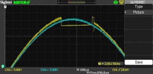
That green trace is horrible.
I don't think a properly built amp does that as it comes out of clipping.
I don't think a properly built amp does that as it comes out of clipping.
Hi Andrew,
They can if the amps "sticks" during clipping, then you get odd recovery waveforms as the feedback loop closes again. Don't forget that during clipping, the feedback goes open and no longer represents what the output stage is doing.
-Chris
They can if the amps "sticks" during clipping, then you get odd recovery waveforms as the feedback loop closes again. Don't forget that during clipping, the feedback goes open and no longer represents what the output stage is doing.
-Chris
Hi reedcat,
Bias will not affect this. Your gain is different between channels assuming the amplifier is working properly.
Look carefully at the values of the feedback resistors. I always use close tolerance metal film types for this with the smallest tempco I can find.
-Chris
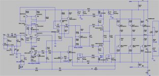
I assume these are feedback resistors going into input stage that I should be looking at, right? R6/R3 each 33k at the schematic.
Also, earlier comments mention adding baker clamp diode to prevent sticking at clipping. Are these the pair of D4/D5 connecting output and power supply rails?
The anti-sticking diode is across Q7/8.I assume these are feedback resistors going into input stage that I should be looking at, right? R6/R3 each 33k at the schematic.
Also, earlier comments mention adding baker clamp diode to prevent sticking at clipping. Are these the pair of D4/D5 connecting output and power supply rails?
It has to be rated for full rail to rail voltage. In your case that will be 2*67Vdc +10% for mains voltage variations.
Just found ostripper's comment on baker clamp diode. It goes between the output side of C8 (where C8 meets R31 and R28) and the Base of Q9 (where C7 meets Q9's base). It is marked D3 on this schematic (attached).
diyAB Amp - The "Honey Badger"
I am not sure if my PCB has it. Does anyone know where I can find the latest schematic for the board on sale? My BOM lists D8/D9 but I don't see them on the schematic listed on the DIY store front or in the schematic included in build guide.
Edit1: I found the latest schematic. It is that little image at the store front. The best way to look at it is right click and save it as an image file. Baker clam is marked at D10. My BOM doesn't have it so I probably don't have it in the PCB which explains the strange shape of the clipped sine wave
Edit2: I found the spot where the diode should be on my PCB. It is marked as "D-BC (option)". The spot is empty. I didn't fill it since the build guide doesn't mention it and the BOM doesn't have it.
Attachments
Last edited:
- Home
- Amplifiers
- Solid State
- diyAB Amp - The "Honey Badger"