Hi guys,
I finished my honey badger and I am starting it up now:
- Power supply +/50 Volt lab supply with 15000µF/rail extra.
- Bias current very stable over temperature, from startup to hot after some full power testing 21 to 23 mV. Perfect.
- DC offset remains 0-2 mV from hot to cold.
- 93V peak to peak just before clipping with a 4 ohm dummy which is about 270 watt.
So far so good but... I do have the same clipping behaviour as mentioned in post 570. I didread the following posts but didn't find a solution for this behaviour. Is there one and if so where can I find it?
Thanks in advance for your time and help.
All amplifiers clip when you apply too much signal.
The ONLY solution is to apply less signal.
The ONLY solution is to apply less signal.
Hi guys,
I finished my honey badger and I am starting it up now:
- Power supply +/50 Volt lab supply with 15000µF/rail extra.
- Bias current very stable over temperature, from startup to hot after some full power testing 21 to 23 mV. Perfect.
- DC offset remains 0-2 mV from hot to cold.
- 93V peak to peak just before clipping with a 4 ohm dummy which is about 270 watt.
So far so good but... I do have the same clipping behaviour as mentioned in post 570. I didread the following posts but didn't find a solution for this behaviour. Is there one and if so where can I find it?
Thanks in advance for your time and help.
If you have the <V2.3 boards , a high voltage - low reverse leakage diode between
Q10 collector (A) and Q9 base (C) ... (A/C=diode).
Version 2.4 has the "D-BC" pads - for the diode.
Source the best diode you can find ... pA to low nA reverse leakage , diode might see that full p-p ..... so 200V minimum reverse voltage rating..
That should solve clip. The other method is don't clip.
Funny thing , yesterday Doug Self basically denied that his/this "blameless"
has a very "nasty" overload behavior. Here , in the real world ... we see it.
😀😱 whoa !!
PS - Self has the full transistor clamp to mitigate saturation in one of his examples -
- he must know !
but that still allows a short "spike" of saturation unless you use a device that
is much faster than the VAS devices. Also , the main CCS still saturates a little.
There is a active baker clamp method , but it would add undue complication.
The diode is sufficient to preserve both amp and speaker (tweeter).
OS
Yes off course they do, they get stuck to the power rails.
But the problem is that there is an osclation just before clipping and the clipping itself is not properly. In case of a normal clipping the top of sine wave is cut of and so you have a sine wave with a flat piece on the positive and negative side of the sine.
In my case the positive side clips earlier then the negative side and not flat. I have build already some amplifiers and normaly the clipping is almost equal on the positive and negative side and certain flat. Just take a look at post 570, I have exactly the same behaviour.
Thanks Ostripper for your reply, my previous reply was to Andrew T but in the time I was writing it your reply came in.
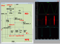
spike and oscillation ....
I know about this , too. TMC "aggravates " this as the output is fed back to a
already saturated Q10.
This is why the diode is best - there are some real fast diodes out there that
can actually clamp as fast as Q10 can saturate. Using our ksa1381 , it's
hard to find many faster clamp transistors - like in Self's book example.
OS
would a small, high fT, To92, or smd, transistor wired as a diode do for a fast Baker clamp?
Wow . never thought about that ! Ok , just simulated it. Electrically , every
B-C connected NPN I tried clamped as good as a diode.
But , THD20K rose to .01-.02%. So your typical transistor must have considerably
higher reverse leakage than that of a diode junction.
OS
Last edited:
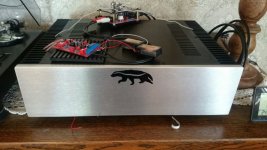
A finishing touch. 🙂
That amp is cute ! That is surely THE badger - A+++ !
OS
yet W.Jung in one of his papers when looking for a very low leakage diode suggested a transdiode. He actually specified a particular device.Wow . never thought about that ! Ok , just simulated it. Electrically , every
B-C connected NPN I tried clamped as good as a diode.
But , THD20K rose to .01-.02%. So your typical transistor must have considerably
higher reverse leakage than that of a diode junction.
OS
Need to try and find the paper, maybe some are better than others.
yet W.Jung in one of his papers when looking for a very low leakage diode suggested a transdiode. He actually specified a particular device.
Need to try and find the paper, maybe some are better than others.
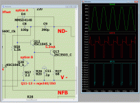
But not with a TMC compensated amp.
(below 1) , a transistor clamp produces a little negative resistance right when
the transistor clamps the saturation. This is just enough to kill the phase margin
for a few uS and give a short burst of oscillation.
(below 2) , the diode is fast enough to just shut things down faster than the
VAS device can saturate ( no "burst").
This does not happen on a standard miller compensated "blameless" , or
is you use a transistor clamp that is the same as the beta enhancer device.
Jung's "transdiode" might of worked for a slower MJExxx type VAS , or
non TMC setup ..... but not on these fast fairchilds.
Also , the diode's reverse breakdown is better defined than the transistor
in a "transdiode" arrangement. - https://www.onsemi.com/pub/.../AN1628-D.PDF
The more typical transistor clamp (below 1) , is never reversed (B-E).
PS - the blue plot is what happens to the VAS CCS , BTW.
OS
Attachments
Last edited:
option B seems to cause the oscillation. that was discussed a few weeks ago.
option A seems to give that pulse, but no oscillation.
What operating conditions causes either option to turn on the protection?
Is it simply voltage clipping, or does some other condition have to apply, like excessive VAS current due to a load?
W.Jung was not using the transdiode in a power amplifier, it was a completely different duty.
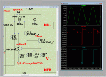
Forgot to show , if Q28's saturation characteristics match Q12's - TMC + the
transistor clamp works as well as the diode (below).
Tried to show this to Mr. Self ....who did not acknowledge this as a "blameless"
errata - then backpedaled and said "just don't clip it". Never explored the TMC
aspect , either. Good thing I don't listen , huh ?
OS
transistor clamp works as well as the diode (below).
Tried to show this to Mr. Self ....who did not acknowledge this as a "blameless"
errata - then backpedaled and said "just don't clip it". Never explored the TMC
aspect , either. Good thing I don't listen , huh ?
OS
Attachments
option B seems to cause the oscillation. that was discussed a few weeks ago.
option A seems to give that pulse, but no oscillation.
What operating conditions causes either option to turn on the protection?
Is it simply voltage clipping, or does some other condition have to apply, like excessive VAS current due to a load?
W.Jung was not using the transdiode in a power amplifier, it was a completely different duty.
Voltage clipping , my EF3 is a VERY minimal load. But even the mA or two
that the Badger EF2 might draw at load would not be a factor.
As you see , it is the timing of the clamp that makes a difference. Either method
is quite flawless as described in self's book (typical miller compensated blameless).
Edit - both clamping methods were perfected on actual slewmaster tests with the real amp
driving real loads.
OS
Last edited:
I do that on all my amps. Just did my 4 slewmasters like that , 100%.
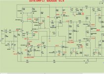
To do the badger , split R36 into two 68R -82R resistors in series. from the center
of the two , take R6's feedback signal. On the badger PCB , this would
just be as simple as each 68R soldered to the output rail.
What you have is a small amp , with just the drivers as outputs. read across Q14/15 (emitters)
OS
Apologies if this sounds lame. I'm in the middle of the build and have some Q's.
Could you please elaborate how this is done. Which center are we tapping the connection ? R6...feedback signal, what /how ? Solder just the 68R, what happens to the 82R, where does that go ?
Apologies if this sounds lame. I'm in the middle of the build and have some Q's.
Could you please elaborate how this is done. Which center are we tapping the connection ? R6...feedback signal, what /how ? Solder just the 68R, what happens to the 82R, where does that go ?
Picture = 1000 words (below)😀 .
R36tempa/ tempb keep the driver current at @ 8ma. they temporarily
connect to output. Read about 1.1V between the driver emitters ,
any connected output will be just short of conduction (safe).
You will also know the rest of the circuit works before you solder in
any high current semi.
PS - I'm about to actually do this on 2 new output stages.
OS
Attachments
Here is a picture (2000 words). You can leave the badger 150R driver resistor
in , just use two 1K resistors across the 150R (R36) , (the middle of them) fed back to output.
Shown is the exact setting of what standard a NJW0281/0302 pair will require
across the 150R for 60ma per device final bias (1.138v).
Amp pictured is nearly the exact same as the badger. In this loopback mode ,
about 22-25ma per rail will be drawn. (8 ma drivers- 15ma+ VAS/input stage).
This is how I get every single one before I load the OP devices.
Vbe can be hit with the flame of a lighter of even a finger touch to see if
thermal compensation is working. All other input stage and current source
operating voltages can be checked as well. Offset can be set close , but you need
the low Z of the real output devices to finalize.
OS
Attachments

Last edited:
- Home
- Amplifiers
- Solid State
- diyAB Amp The "Honey Badger" build thread