Hi Rick,I have opened up the solder mask on traces to get more plating on them. If the pcb is wave (or done by hand) soldered, it builds up more plating, so you have a lower resistance trace that will handle more current.
Thanks for trying to help out.
I don't think we need to do that. There is no rush to finish this pcb.
Let's just wait for OS to submit the BOM and possibly some direction on trace width. Hopefully he is happy with the plan from post #535 once he reads post #525 and #527
OS wasn't a fan of removing the solder mask nor am I, it's a bit bodgie.
Last edited:
I think is a very good option😉I have opened up the solder mask on traces to get more plating on them. If the pcb is wave (or done by hand) soldered, it builds up more plating, so you have a lower resistance trace that will handle more current.
I don't have alot of time during the week, but I did managed to sit down and put a bit of thought into this problem.
This is what came up with.
I will need to check over a few other things once I receive the ltspice file and BOM from OS.
I will have at least a day free on the weekend to continue so hopefully OS has the BOM complete by then.
View attachment 944243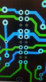
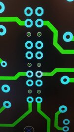 View attachment 944242
This is what came up with.
I will need to check over a few other things once I receive the ltspice file and BOM from OS.
I will have at least a day free on the weekend to continue so hopefully OS has the BOM complete by then.
View attachment 944243

 View attachment 944242
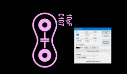
Not all , 470p is 7.9mm ... harder to find 500V 470p is 5.9mm.
68,100,56pF are 5.9 .. generally.
OS
uhmm got it this macro cap I'm gonna attached here and send it to Stuart yes 😀
Attachments
Moving to NY...
Stuart , send me your latest version (with the mica macro's). I will try
to finish ALL this by 4/28 , then I'm offline for up to a month.
I did find , doing the BOM ... that C101,105 (multiplier)/C3,IPS is 2mm LS.
Some other 10uF's are 2.5mm ... 22uF/100V is generally 2.5mm LS.
So , the choice of 22uF would be generally helpful for all 3 components.
Space is available for all 3. Make a macro with 2/2.5mm LS. A wider choice
is then possible.
The bigger 47/100uF 100V caps (C102,103,106,107 are always 5mm LS),
all brands. While I would like a 220uF option , no space.
With a cap multiplier , the gain of the transistor is a direct multiplier of the
caps value .... so, a semi with twice the gain would equal a 220uf(for 100u).
47uF with a 400 gain semi would equal roughly 220uF @ 100 ....
The biggest caps , C115/117 are best kept as they are.
ALL the brands are 7.5mm LS ... some are pretty tall !!
With Nichicon , one could go up a size to 680uF (UPJ2A681MHD1CA).
PS - another option if you use 65V and under rails is ( UPJ1K102MH),
which is a 1000uF !!! @ 80V unit.
OS
Last edited:
I don't have alot of time during the week, but I did managed to sit down and put a bit of thought into this problem.
This is what came up with.
I will need to check over a few other things once I receive the ltspice file and BOM from OS.
I will have at least a day free on the weekend to continue so hopefully OS has the BOM complete by then.
View attachment 944243View attachment 944245View attachment 944244View attachment 944242
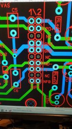
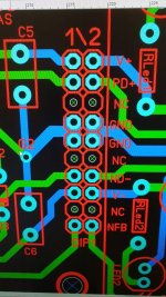
Ain't (I know) a problem . PD+/ND- are at NANO amps/@ 110v p-p.
G2 or the rails , which draw as low as 15mA.. would not "see" anything.
PD+/ND- are the (very) high Z traces. This , looking at 100's of OEM EF3's,
is a rule they all follow(my traces). They never run these traces anywhere near a higher current return.
They are ideal as they are between the clean C mult. outputs and G2.
An example of where you would NOT want to run these traces would be
like close to C103/4 "very dirty" (output/driver ripple decoupling).
PS - NFB , on the other hand ... is super low Z at mA's. While not high current ,
a CRO probe would possibly show a signal within mm's of this trace without even touching
it (at 100Vp-p).
OS
Last edited:
>Moving to NY ...
Many people move out of NY these days, not moving in 🙂
Especially out of NYC...
Many people move out of NY these days, not moving in 🙂
Especially out of NYC...
>Moving to NY ...
Many people move out of NY these days, not moving in 🙂
Especially out of NYC...
Yup, my thoughts as well 🙄
I hope you have a safe and drama free move.
Welcome to NY!
Last edited:
Thank you...
I need to step in and say thank you 🙂
Pete, you're doing a great job for DIYA, the badger was a lovely child - but this project really is a mature masterpiece. The community drives it to perfection with a superb pcb layout ending in a fool-proof construction kit for a tremendous amplifier.
Don't have that much time I can spend on contributing, even hard to keep track of this thread - but it is worth it. Can't await seeing this beauty alive 😀
Best,
Holgi
>Moving to NY ...
Many people move out of NY these days, not moving in 🙂
Especially out of NYC...
I will miss the pretty mountains of Tenn. , but (upstate)NY is home.
PS - Not NYC , visited once .... never again.
OS
I need to step in and say thank you 🙂
Pete, you're doing a great job for DIYA, the badger was a lovely child - but this project really is a mature masterpiece. The community drives it to perfection with a superb pcb layout ending in a fool-proof construction kit for a tremendous amplifier.
Don't have that much time I can spend on contributing, even hard to keep track of this thread - but it is worth it. Can't await seeing this beauty alive 😀
Best,
Holgi
Thank you ,sir.
Hopefully I can convince Jason of this.
OS
I can't move nowhere I'm in Puerto Rico 😀 good travel OS 🙂
Yeah you could , same as I could go to PR .... to see the cool caves near you.
Airplane ??? 😀
Edit - Bosque Estatal de Guajataca - Neato !!
OS
Ain't (I know) a problem . PD+/ND- are at NANO amps/@ 110v p-p.
G2 or the rails , which draw as low as 15mA.. would not "see" anything.
PD+/ND- are the (very) high Z traces. This , looking at 100's of OEM EF3's,
is a rule they all follow(my traces). They never run these traces anywhere near a higher current return.
They are ideal as they are between the clean C mult. outputs and G2.
An example of where you would NOT want to run these traces would be
like close to C103/4 "very dirty" (output/driver ripple decoupling).
PS - NFB , on the other hand ... is super low Z at mA's. While not high current ,
a CRO probe would possibly show a signal within mm's of this trace without even touching
it (at 100Vp-p).
OS
Hi OS, Attached are the latest files.
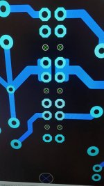
If we try and develop clearance between traces with high potential difference between them by using alternating sides of the PCB this may solve the creepage problem. I also recommend reviewing the Pad sizes using my calculator. The outer ring it very large in some instances and 1mm inner ring is a little large for 1/4 watt.
Attachments
Hi OS,
Please don't feel pressured to finish this before going to NY.
I'm sure most of the guys on this thread are willing to wait for are optimized PCB.
Stuart's idea of having traces with high voltage on alternate sides of the PCB is good.
Good luck in the move!
Please don't feel pressured to finish this before going to NY.
I'm sure most of the guys on this thread are willing to wait for are optimized PCB.
Stuart's idea of having traces with high voltage on alternate sides of the PCB is good.
Good luck in the move!
You don't need to use a 2 X 10 position DIP 1 interface. NFB and PD+/ND- are quite optimized.
???
PS - Slewmaster actually used the "DIYaudio fanatic" method of IPS NFB
delivery. This is running a shielded wire from G1/NFB output rail to the
IPS NFB through-hole. These two through-hole's could be 1mm proper
pads (leave the interface NFB jumper off) and the "fanatic" option would live again !
Edit , you know what ... a 10 pin 2 X DIP1 is alright. Overkill , but just as available.
OS
Last edited:
- Home
- Amplifiers
- Solid State
- DIYA store "Wolverine" (Son of Badger) .... suggestions ??
