The Cornell-Dubilier Mica from RS are also 5.9mm, although there is smaller pitch 3.6mm in some values, but not all.
Attachments
Last edited:
Here's the 2 silver mica's I chose for the BOM (almost done).
Emitter Resistors R120-125a/b are either 2 X .47-.5R per emitter.
Vishay PR02 or any 15mm LS will do.
Single Resistors could be those KOA 15mm LS wirewound ceramics Thimios
posted.
OS
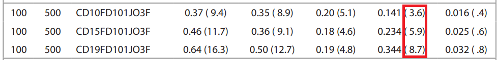
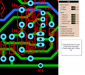
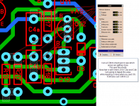
C4a - 100pF silver mica - CDE - 5.9mm LS - CD16FD101JO3F
C4b - 470pF silver mica - CDE - 5.9mm LS - CD15FD501JO3F (500pF)- 5.9mm CD19FD471JO3 470pF (7mm LS)
Emitter Resistors R120-125a/b are either 2 X .47-.5R per emitter.
Vishay PR02 or any 15mm LS will do.
Single Resistors could be those KOA 15mm LS wirewound ceramics Thimios
posted.
OS
Last edited:
Here's the 2 silver mica's I chose for the BOM (almost done).
Emitter Resistors R120-125a/b are either 2 X .47-.5R per emitter.
Vishay PR02 or any 15mm LS will do.
Single Resistors could be those KOA 15mm LS wirewound ceramics Thimios
posted.
OS
Hi OS,
Can you please include the lead pitch on your bom for the caps that way I can check the layout is suitable.
What about the pads for the holes. Do you mind if I reduced the ones for 1/4w, 1/2w, small caps to 0.9mm inside and 2.0mm outside were they are currently 1mm x 2.4mm?
I'll leave the output transistors emitter resistors as is.
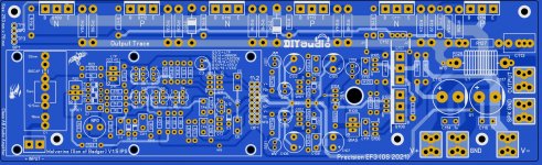
Stuart's last V1.5.9 with upgrades.
-R20/21 tweaked
-ground moved away from R21-C4a/b.
-small inner IPS trace tweaks.
-R25 will bias - for a positive response (offset). So clockwise/counter might
not matter. A builder would turn it one way or the other while watching
his DMM. +mV or - ... who cares. Having it point (down) matters.
-Repositioned all the semi EBC's/label's. Spooky is this way.
All of Stuarts other tweaks are golden.
OS
Attachments
-R20/21 tweaked
-ground moved away from R21-C4a/b.
-small inner IPS trace tweaks.
-R25 will bias - for a positive response (offset). So clockwise/counter might
not matter. A builder would turn it one way or the other while watching
his DMM. +mV or - ... who cares. Having it point (down) matters.
-Repositioned all the semi EBC's/label's. Spooky is this way.
All of Stuarts other tweaks are golden.
OS
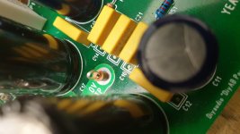
Hi OS,
Thank you for taking a look at the file and sending it back.
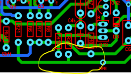
I see what you have done to maintain clearance around those high voltage areas.
I found that a little more needed to me done as other pads and traces in that area were still very close.
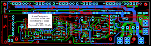
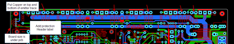
Please review the images to see what I have done.
I don't believe that any other traces need tweaking anymore and we should try and focus on more productive things.
Juan helped out and I think as far as that goes we are good to go.
I will review the pad hole sizes, LS and silkscreen once I see your BOM.
Attachments
Last edited:
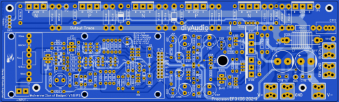
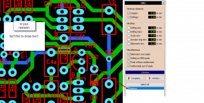
Hi OS,
Please take a look at this, There maybe a problem with creepage and clearance in some areas. I have noted down one for you to look at.
I could check the board but is a lot of work. You need the LT spice schematic and you need to look at the worst case for all adjacent traces. Takes a long time.
Any ways I have included my creepage circle macros which I use as a guide to determine if I have the required clearance.
I have also attached my latest file.
Attachments
Last edited:
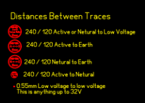
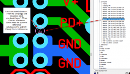
The biggest area to concern yourself with creepage distance is around the feedback trace, particularly around the proximity of the high voltage rails. Voltage to ground is maximum 60V, which isn't really a big deal. Feedback can swing close to rail voltage, so it can approach 120V (in theory with a perfect amplifier). The area at the bottom of R20 is really the only part that concerns me with the input stage. R19 is connected to the negative rail. Everything is too tight there.
Attachments
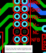
PD+ and ND- to rail voltage is another area of concern, but they are at least current limited. Maybe consider switching the pin header pads to a narrower oval shape. I normally used a .050" round pad but I know new builders prefer larger pads.
What are the hole sizes of those TO92 transistors. Big holes = big pads
Not every track has to be the same thickness
Not every track has to be the same thickness
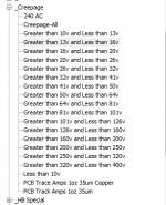
For pcb layout IPC2221.
in pdf page 51 and 52/131, on page bottom marked 39 and 40.
http://us.jetpcb.com/Cht/Document/ipc-2221all.pdf
in pdf page 51 and 52/131, on page bottom marked 39 and 40.
http://us.jetpcb.com/Cht/Document/ipc-2221all.pdf
Hi Guy’s,
Maybe we can work out a plan to move forward with this PCB.
One possible way that I have used before is.
1. Use LTspice and set the circuit parameters for the worst case.
a. So for Example 70v and 4 ohms
b. OS Please upload the LTspice file.
2. We then size all traces to have at least 1.5 – 2 times that load rating. While keeping the minimum trace width to 0.40mm.
3. We then use the BOM that OS is working on and my PCB pad calculator (attached) to size the pads accordingly.
4. We then check the creepage. Some area’s won’t take long and other area’s will take some time.
What do you guy’s think?
Attachments
Last edited:
2. We then size all traces to have at least 1.5 – 2 times that load rating. While keeping the minimum trace width to 0.40mm.
A 0.4mm/35um pcb track can carry 1.6amps, to carry 1.5-2 times the rating the track would need to be 0.9mm-1.5mm wide.
Sorry Indiglo,A 0.4mm/35um pcb track can carry 1.6amps, to carry 1.5-2 times the rating the track would need to be 0.9mm-1.5mm wide.
That's not what I meant. Sorry that I was not clear. What I meant to say was if we see from spice simulation that the trace will carry 100mA we the multiple that by between 1.5 & 2. Round up to the nearest 0.1mm. So let's say 200mA we the look at the required trace width. Looks like its less than 0.1mm. But we have decided that 0.4mm is the narrowest trace. So use 0.4mm.
Hope that clears up the proposed process.
Last edited:
Nice project. But I deeply regret that you discarded the helper Q5 for the current mirror. I did not really understand this decision of yours. Therefore, may I rewind back to the CM helper Q5 story? I am coming late, I know.
I am theoretically (and maybe also practically) interested in this kind of helper-transistor enhanced CM. Also because this topology comes along with an extended benefit, e.g. described by S.Groner:
S.Groner describes how a helper transistor is of great worth. You instead write about "more trouble than it's worth" coming along with a helper Q5. So what exactly do you mean by trouble?
I am theoretically (and maybe also practically) interested in this kind of helper-transistor enhanced CM. Also because this topology comes along with an extended benefit, e.g. described by S.Groner:
Samuel Groner said:...
Better cancellation and more freedom for VAS biasing is achieved with theEFA mirror (figure 1). If R5 is chosen such that Q1 and Q2 are operated atequal collector voltage and R3 and R4 have equal value the error introducedby the base current of Q5 is cancelled with the base current of Q6. Overallthis topology leads to very good input stage balance and offers low drift (seee.g. [1]).
...
... Q5 seems to be more trouble than it is worth ...
S.Groner describes how a helper transistor is of great worth. You instead write about "more trouble than it's worth" coming along with a helper Q5. So what exactly do you mean by trouble?
Last edited:
Sorry Indiglo,
That's not what I meant. Sorry that I was not clear. What I meant to say was if we see from spice simulation that the trace will carry 100mA we the multiple that by between 1.5 & 2. Round up to the nearest 0.1mm. So let's say 200mA we the look at the required trace width. Looks like its less than 0.1mm. But we have decided that 0.4mm is the narrowest trace. So use 0.4mm.
Hope that clears up the proposed process.
Many of the older designers (Richard Marsh for example) have found distortion is lower with wider traces in the input stage. This was discussed a few times in the Slewmaster thread. Best to stay with the 1mm trace width for a through hole design.
Marsh also started using Servos, does that mean you guys going back to the servo version. Offcourse everything a compromise in the end.
Distortion using a 1mm track vs 0.5mm track is measurable in a functional working amplifier connected to an actual speaker. If so why 1mm and not 1.5mm. Where did 1mm become the gold standard
Distortion using a 1mm track vs 0.5mm track is measurable in a functional working amplifier connected to an actual speaker. If so why 1mm and not 1.5mm. Where did 1mm become the gold standard
Last edited:
- Home
- Amplifiers
- Solid State
- DIYA store "Wolverine" (Son of Badger) .... suggestions ??