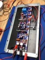
When you get everything together, you need to make the adjustments with the top cover sitting on top. It took me most of a day to get it tweaked.
I'm glad you reminded me. I have to pull the IPS board to recover that resistor as I need to install it in the other channel. I lowered the bias back to zero. I believe the board was pulling something like 485 mA.Perfect and keep an eye on it, it may change in 30 minutes or so. For this test, I think you are done. Lower the bias back down to zero and you are ready for your final power supply. Don't forget to remove the resistor in parallel with R17 before applying your final power supply. Also, how many milliamps was the 1st board pulling, write it down, the 2nd board should be close.
Thanks,
J

Ok, this process is similar to the F4 and F6 amplifiers I built. It's all about the thermal environment inside the chassisWhen you get everything together, you need to make the adjustments with the top cover sitting on top. It took me most of a day to get it tweaked.
J
Hello again,
I am now doing initial testing without output transistors on EF3-4 V 4.0's other channel using a 30V bench supply.
I brought the voltage up slowly and the first thing I noticed is D10 and D11 did not light as they had in testing channel 1. This surprised me, but I carried on.
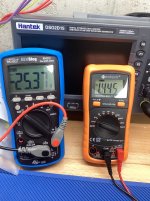
Output voltage across R111A and R111B measured 758 mV.....exactly as the first channel measured.
I was able to adjust R11 to get 5.0 V so that the proper current is established for the long tail pair.
I measure 593 mV between TP3 and TP4 which just about what the other channel measured.
Voltage between TP-105 and the positive rail and TP-106 and the negative rail were 1.454 and 1.528 V....almost identical to the first channel tested.
My problem is that I cannot zero out the DC offset. It measured a whopping -25.37 V. Adjusting R25 I hit a point where it goes from that negative voltage to a +28.36. No amount of tweaking gets around this issue.
Is this somehow related to D10 and D11 not lighting....or do they not light at 30.0 VDC because here simply isn't enough voltage? What else could I have done to not be able to adjust the DC offset?
I was able to set the output bias to 1.4-1.5V using R109, and it remained stable.
I am now doing initial testing without output transistors on EF3-4 V 4.0's other channel using a 30V bench supply.
I brought the voltage up slowly and the first thing I noticed is D10 and D11 did not light as they had in testing channel 1. This surprised me, but I carried on.
Output voltage across R111A and R111B measured 758 mV.....exactly as the first channel measured.
I was able to adjust R11 to get 5.0 V so that the proper current is established for the long tail pair.
I measure 593 mV between TP3 and TP4 which just about what the other channel measured.
Voltage between TP-105 and the positive rail and TP-106 and the negative rail were 1.454 and 1.528 V....almost identical to the first channel tested.
My problem is that I cannot zero out the DC offset. It measured a whopping -25.37 V. Adjusting R25 I hit a point where it goes from that negative voltage to a +28.36. No amount of tweaking gets around this issue.
Is this somehow related to D10 and D11 not lighting....or do they not light at 30.0 VDC because here simply isn't enough voltage? What else could I have done to not be able to adjust the DC offset?
I was able to set the output bias to 1.4-1.5V using R109, and it remained stable.
Attachments
Do you have the temporary parallel resistor in place on R17? J103 installed?
Do you have the negative feedback solder bridges installed? Also the TMC jumper
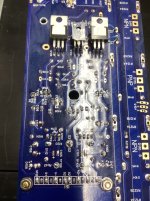
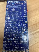
Pic is too blurry to identify any physical errors. But the offset immediately swinging from almost full rail to opposing rail is indication something is not right.
Do you have the negative feedback solder bridges installed? Also the TMC jumper
Pic is too blurry to identify any physical errors. But the offset immediately swinging from almost full rail to opposing rail is indication something is not right.
Last edited:
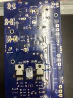
R17 is installed, and I measured the resistance and it matches what I had on the other channel. The J103 jumper is in. The TMC jumper is in. I have 3 negative feedback bridges soldered on EF3-4 (3rd Group Buy) including Route 2, but not Route 1 (as I assumed they were mutually exclusive).
Could I have reversed those diodes at D10 and D11? Would that cause a problem with DC offset?
John
Could I have reversed those diodes at D10 and D11? Would that cause a problem with DC offset?
John
Attachments
Your NFB connection appears to not be closed as I suspected. See here

Easy to check the diodes in circuit. Use a multimeter in diode mode, and you can even see the LED light up. Here's a handy excerpt attached from the upcoming build guide. (currently draft)

Easy to check the diodes in circuit. Use a multimeter in diode mode, and you can even see the LED light up. Here's a handy excerpt attached from the upcoming build guide. (currently draft)
Last edited:
I'm right with you. Just checked the diodes. D10 is reversed assuming that the "A" next to "D10" on the underside of the pcb indicates Anode. I never saw diodes marked like this before. What do those pairs of arrows signify?
Is this causing my offset issue?
J
Is this causing my offset issue?
J
The NFB bridge not being connected I'm almost certain is causing your offset issue.
The LEDs being backward is possibly another issue. Arrows on a diode symbol in a schematic mean the diode is an LED. Arrows on the PCB also indicate the diode is meant to be an LED. In the absolute most basic possible terms, a diode and an LED are the same thing, one just emits light as voltage drops across it, as a nice way to show you that part of the circuit is functioning. (there are many more reasons but lets not get into that here)
Did you get the LEDs to light? If meter in diode mode, the positive on "A" and negative on the other terminal should make the diode light. If it lights the other way, its backwards. If it dont light, she ded.
Last edited:
Damn! I missed it. I've got solder on the pads, but they are open!
I am going to have to cut that diode out. It won't drop. I tried adding solder and using the Hakko Desoldering Iron, but it won't give. I have an LED to replace it.
Mainstream, you've got eyes! I'm heading for cataract surgery in the Fall (really).
Thanks,
John
I am going to have to cut that diode out. It won't drop. I tried adding solder and using the Hakko Desoldering Iron, but it won't give. I have an LED to replace it.
Mainstream, you've got eyes! I'm heading for cataract surgery in the Fall (really).
Thanks,
John
Best of luck John with everything, lets get this amplifier running before then eh! 👍
Make absolutely sure you need to take out LEDs first. If you do need to remove the LEDs, they will come out easier if you use a normal soldering iron to bend the legs up vertical first (it appears as though they are bent to help with positioning during install which is okay, but it will make it hard for a desoldering tool to fully remove the solder).
Once it's out you can test it again for function but soldering it back in can be risky as there's only so many heat cycles they can take from the iron (as with all parts). For what it's worth, if you don't have spares, you don't need to source the BOM LEDs if you don't want to wait for mouser. Any 3mm RED LED from a local electronics store will do.
Last edited:
I put it all back together. All 6 LEDs light up. I was able to zero out the DC offset. There's no AC between the output and speaker ground.
Tomorrow I'll install the outputs.
Thanks Mainframe!
John
Tomorrow I'll install the outputs.
Thanks Mainframe!
John
- Home
- Amplifiers
- Solid State
- DIY Class A/B Amp The "Wolverine" build thread