It has built in "natural" current limiting to offer some protection for the output transistors from accidental shorts.Does this Amp have built in speaker protection?

The power amp has a gain of 27, so an input of 1.5v peak to peak will give an output of 50v p-p approx or about 100W in an 8 ohm load. The input Z is approx 100k.Novice here, & yes I realize an AVR is not the "cleanest" source, although I'd argue THD+N of 0.001 is clean enough;
What is the input impedance of the wolverine - will it be hampered by the (speculative) high output impedance of a Denon X3700H AVR @ around 1.2kohm?
And also the input sensitivity or gain figure - just to workout power output at say 1 to 1.5V input.
That is the DC resistance. The AC impedance is 100kohm||(1kohm+27kohm)=~22kohm.The power amp has a gain of 27, so an input of 1.5v peak to peak will give an output of 50v p-p approx or about 100W in an 8 ohm load. The input Z is approx 100k.
Jeremy
@mainframe99The power amp has a gain of 27, so an input of 1.5v peak to peak will give an output of 50v p-p approx or about 100W in an 8 ohm load. The input Z is approx 100k.
Due to R26 & C10 the Closed Loop Gain is closer to 26.5
@mainframe99
The PCB does have a speaker protection header for ease of connection. It monitors the emitter voltage of both the NPN & PNP output transistors. You can connect this to your own speaker protection PCB.
Thanks guys, appreciated. Though not my only application, it should work fine with the 1.2kohm out AVR.
Two question to designers of this amp, I know it's too late for that but why didn't you include SOA protection circuitry as an option? Those purists who would not like it simply would not populate that section with components.
The other question is why two boards? Any special reason for lifting that section?
Probably explanation for that was included at the development stage but I missed that.
Thank you,
cheers,
The other question is why two boards? Any special reason for lifting that section?
Probably explanation for that was included at the development stage but I missed that.
Thank you,
cheers,
You could simply add SOA protection via the supplied headers. IPS is on a second board for simple exchange for another IPS.
It wasn't planned from the beginning so board space wasn't reserved. We would need to make the the pcb bigger to implement SOA protection as currently there is no more room. SOA protection can be tricky to implement also because you don't want it to falsely trigger on normal signals. Honestly a lot of diy falls short in this area.Two question to designers of this amp, I know it's too late for that but why didn't you include SOA protection circuitry as an option? Those purists who would not like it simply would not populate that section with components.
The other question is why two boards? Any special reason for lifting that section?
Probably explanation for that was included at the development stage but I missed that.
Thank you,
cheers,
Jeremy
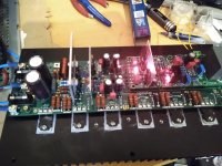
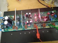
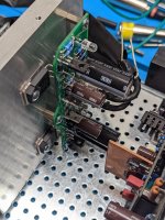
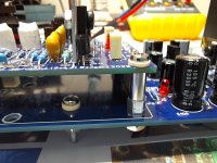
Made a little progress ☺️. The first board went together like a dream. The second board isn't entirely cooperating. D10 and D11 briefly turn on then off. Also have almost full rail voltage at the output. This is without output transistors on the second (none working) board. The pictures are of the working board. I'll post the none working PCB tomorrow if I can't figure it out. 🙂
edit - looks like I missed one of the solder bridges on the NFB trace... the pads are tinned but no bridge.
edit - looks like I missed one of the solder bridges on the NFB trace... the pads are tinned but no bridge.
Attachments
Last edited:
Has anyone ordered KSC3503E units from MOUSER/DIGIKEY/NEWARK? If so could you report the average HFE? Also anyone with MJE340 units which measure HFE around 150? I have 80+ MJE340/MJE350. The MJE350 all measure around HFE150, but all the MJE340 units measure around 90 HFE. Anyone with a source for higher HFE MJE340 or willing to trade a few?
Folks:
Like zlast, I'm having a problem with transistor matching. I'm using TTC004BQ for Q105 and TTA004BQ for Q106, and bought a bunch of both. All of my TTC004BQ transistors measure an hFE of 215 and all of my TTZ004BQ transistors measure an hFE of 309. Is there an easy way to compensate for this disparity, or do I need to find two matched pairs somewhere?
Regards,
Scott
Here is what I found. Also I have 2SC and 2SA which match nice. I also have KSA which do not match as nice to the older 2SC part#. I purchased mine in bulk from rochester electronics, and by bulk I mean I bought 2000 each. My MJE340G where purchase new from mouser. mje340g
Attachments
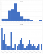

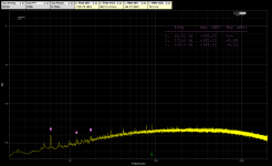
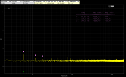
Just a small update, I have started on chassis 2, but I am trying some different options to get the lowest noise floor I can. I also am testing the B2UIA pcb by @LKA . I built one to test and it exceeds the level of my test equipment! Great design. I am also using the MRA by @Bonsai as well. I have some preliminary noise data, but nothing yet with the finished wiring layout. One thing to note is the use of a ground lifter made a HUGE difference on my noise floor measurements.
Attachments
-
 noise20-20k_Aweighted.png78.2 KB · Views: 320
 -
 noise20-20k_unweighted.png70.7 KB · Views: 246
 -
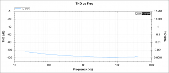 thd vs freq B2UIA.png12.2 KB · Views: 236
 -
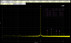 thd2 B2UIA.png100.4 KB · Views: 327
 -
 PXL_20220621_202725512.jpg539.4 KB · Views: 348
 -
 PXL_20220621_202740249.jpg679.3 KB · Views: 370
 -
 PXL_20220621_202801063.jpg466.4 KB · Views: 332
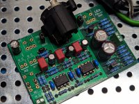
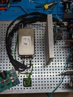
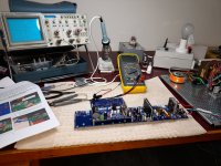
I have finally scored enough time to start testing my build.
First board only to date and the preliminary tests only so far but it works. To get this far I had to build a bench supply so re-purposed a recovered transformer with added switched secondaries giving either 50Vac or 34Vac plus a bridge rectifier and a couple of capacitor banks all mounted on one of the DIYStore base plates. And a stroke of good fortune had a former Telecom colleague give me his 30 year old Tektronic 2236 scope that he had "acquired" when that branch closed (we formerly worked in the radio branch until some idiot invented fibre optic cables during the 1980's, I left but he moved into broadcast).
Some photos attached to highlight the mounting techniques I used.
Attachments

The Wolverine team, danieljw:
I recommend on page 36 Build Guide add G1 and G2 ground connections to the diagram (or text), danijeljw has it connected on video (IPS board tested in Isolation).
Questions:
I recommend on page 36 Build Guide add G1 and G2 ground connections to the diagram (or text), danijeljw has it connected on video (IPS board tested in Isolation).
Questions:
- during the IPS test in isolation I have a power supply of + -30V and the diodes D10 and D11 do not light up (there is a voltage of 1.4V on them). Build Guide point 15.B states that it may not light when the power supply is less than 35 V. It's alright ? Q11 = KS1381E (Hfe=115) , Q13 = KSC3503D (Hfe=83), can it affect the lighting of D10, D11 ??
- during the IPS test in isolation on DMM3 the voltage fluctuates + - 2mV, is it OK? (oscilloscope test is OK - 2.5Vpp)
@janusz, I suspect I will regret trying to answer this one....but here goes:One question. A friend of mine asked that and I didn't know. He's got Electrocompaniet and loves high DF as high DF better controls speaker behaviour.
What is the damping factor of this amp?
It has not been mentioned in the manual nor on schematics.
Thank you,
cheers,
My understanding is that a class AB, emitter follower, SS, feedback amp is a voltage source having essentially zero source impedance and a meaningless infinite damping factor.
Also that Tube amps with an output transformer on the other hand have an output impedance designed to match the speaker impedance to achieve maximal power transfer, which of course is where and why damping factor became a thing. Possibly a class A, no feedback amp with an output capacitor also has significant source impedance and would need to consider load matching. Because speaker impedance changes with frequency (eg drops at woofer resonance) the amount of power "lost" in high source impedance amps also changes and typically this is most noticeable at the low frequencies approaching woofer resonance.
These days I see DF as a marketing thing of no consequence unless you have transformer outputs.
- Home
- Amplifiers
- Solid State
- DIY Class A/B Amp The "Wolverine" build thread