@soekris
Well, you never know! Perhaps it will be feasible. But if so, it should probably be a mark 2. There are enough open ends at the moment!
@altor
Thanks. That is interesting. I also used the OPA1632 for my AK5394 design. I included a couply of mounting options. On one channel I used DC coupling on the inputs of the OPA1632, driving them from the outputs of an OPA1612. On the other channel I used AC coupling directly from the input connector.
I definitely saw some issues when driving the OPA1632 from another OPA1632 (in the generator output). The distortion was much higher than in other cases.
demian;
yes, please do.
mlloyd1
never mind, i saw you later post and too late to delete this one now.
yes, please do.
mlloyd1
never mind, i saw you later post and too late to delete this one now.
... I tried a passive L/C filter which has two benefits. ... I can dig out the details if anyone is interested.
Last edited:
Your posting also crossed mine....
Shouldn't you assume that ESS can meet the specs ?? The output buffers are pretty critical to meeting specs, so the fft plot itself isn't that useful without buffer schematics....
I meet with Semiconductor guys several times a week. We have a saying- How do you know when a chip vendor is lying? His lips are moving. . . .
Those measurements were using the ESS demo board with its optimized analog design. That's all on their datasheet. The noise in the measurement may partly be due to grounding. I don't remember and i returned the demo boards. At $500/ea they weren't worth keeping.
The LTC part looks interesting but getting it working with available software etc. would be a major development project, more than a normal hobby project. However there may be useful tricks in the applications info for the LTC2378.
The ESS noise floor is constantly changing. I have seen notes on locking the sample rate converter but thats a project. I was really disappointed in the performance of the ESS ADC. It looked very promising on the datasheet. Their support people did not have any ideas either.
I was really disappointed in the performance of the ESS ADC. It looked very promising on the datasheet.
I can say the same about PCM4222

Another detail I just remembered- The AK4490 will have lower distortion on the 44.1 clock frequencies. I discovered this and confirmed it with AKM. It has something to do with internal timings. They chose to optimize for the 44.1 clock frequencies since that is what most music is distributed at.
Hello,
I think also that LTC2378-20 chip (and some others from LT) are very interesting option.
In fact, the complete EVM cost 500€ and include a very complete good software (PScope)
allowing to make comprehensive measurement.
The THD level is comparable to best sigma/delta ADC IC (like AK5394A) and measurement bandwidth is much wider (1Msps). This allow wider possible application range. Of course, not all is pink. Because it's not oversampling ADC, input filtering is more critical.
I really ask me when i will buy one !
ESS ADC chip (ES9102) seemed interesting, but only very parceling infos are available and a NDA must be signed to get full datasheet.
From now some years i don't have seen any design based on this IC with extended measurements results... IMHO, not at all DIY friendly. Really shame.
Frex
@Demian,
Was that at a particular output level (and frequency)?
I measured the distortion at -10dBFS/1kHz a couple of days ago. I did this for 44.1, 48, 88.2, 96, and 192kHz sample rates using the VP-7722A. The results I saw were almost the same. But the read-out was not totally stable. Most results were at -122dB. 44.1 was -123 on one channel and -121 on the other channel. The best result was seen at 192kHz with -122 and -125dB.
That was some time ago and the difference was small but still enough to be consistent, something like 2 dB or so.
I think the chip runs the same internally on all sample rates and just engages some filter stuff/dsp for the slower sample rates.
Related, AKM has a new sample rate converter that does it all including DSD and DSD 2X to everything else. Adding that to a universal audio tester would prove very useful. I do a lot of mixed mode (analog to digital and back) testing and having a good selection of I/Os would be great. Altor's digital box JKGEN - ALTOR AUDIO comes very close (its also very good) but it doesn't solve these issues, necessary for testing things like digital in speakers and bluetooth headphones.
@Demian,
Was that at a particular output level (and frequency)?
I measured the distortion at -10dBFS/1kHz a couple of days ago. I did this for 44.1, 48, 88.2, 96, and 192kHz sample rates using the VP-7722A. The results I saw were almost the same. But the read-out was not totally stable. .
Yes! Exactly!
I have the same experience - the results are not stable, differ from left to right channel and from one pcb to another.
I'm still don't know the reason clearly, but I have seen that THD more depend of a signal level (also duie to ADC) then of the samplerate.
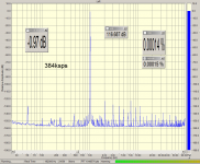
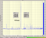
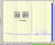
These are the best results I got from my ATDAC-10B (AK4440 based, by the way - the same model 10A, which based on AK4414 in double mono, shows very close results):
Attachments
-
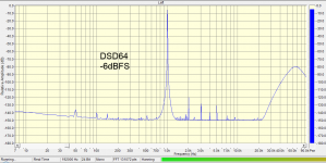 b dsd64 1k fb.png63.9 KB · Views: 1,251
 -
 atd10bb_thd1k_-10db_384_USB.png91.6 KB · Views: 308
 -
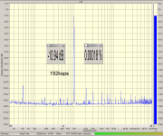 atd10bb_thd1k_-10db_192.png87.3 KB · Views: 286
 -
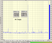 atd10bb_thd1k_-10db_44.png80.7 KB · Views: 287
 -
 atd10bb_thd1k_0db_384_USB.png93.3 KB · Views: 306
 -
 atd10bb_thd1k_0db_192.png89.4 KB · Views: 1,173
 -
 atd10bb_thd1k_0db_44.png79.1 KB · Views: 1,185
 -
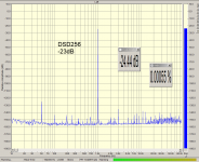 atd10bb_dsd256_-20dB_USB.png89.1 KB · Views: 1,207
 -
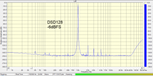 b dsd128 1k fb.png63.6 KB · Views: 1,201
The ESS9112 ADC is not as bad as described here.
The ES9112ADC with OPA1632 input stage and a OPA1641 buffer is direct driven by a ES9018 with a OPA1632 I/V stage without DC blocking capacitors.
If the ADC is synchronized externally over the I2S Clock, then I use a master clock from 60 to 80 Mhz.
The upper limit of the MCLK frequency is about 60MHz. It appears that the digital circuitry can run much faster but the analog portion may have a limitation.
best Thomas
Attachments
@spiri
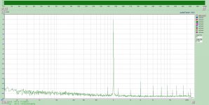
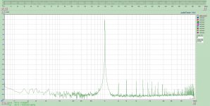
It would be nice to see the spectrum beyond 20kHz.
Yes, we would really love to see FFT's on higher samples rate up to nyquist, that are not in any datasheets....
@altor,
I have now modified one of the channels on my AK5394A design to use AC coupling on the inputs of the OPA1632. But it gave only a marginal change. I get nowhere near the result you have shown in post #63.
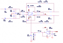
Could you post the schematic of the ADC driver?
Sure, but nothing interesting, all - "text-book":
Attachments
Amazing work, you're the boss!
I soldered the components by hand. No stencil. It probably took me something like 20-25 hours to do so. Excluding the time it took to find the components in different sample kits etc. I used parts from these sample kits for all the uncritical parts. The critical parts, e.g. 0.1% resistors, I ordered from Farnell and Mouser.
I have a Mantis Vision microscope, which helps a lot in the assembly process. Without it, I would have no chance to assemble it by hand. Maybe I could have done it 20 years ago, but not today.
It is a big task to solder it by hand and I have no plans to assemble a second one by hand! But for a first prototype, to verify the performance, it was OK.
Hi Alex,
Thanks for the schematic.
There are a number of differences compared to my OPA1632 circuit:
1. The feedback resistors have much higher values.
2. The 3k resistors connected from the outputs to the negative supply.
3. The filter circuit on the input side.
4. The gain is different.
I have used something very close to the schematic in figure 11 in the data sheet.
I could imagine that especially 1 and 2 above could have an impact on the distortion. I assume that 2 is to let it run in a kind og class-A mode. I used a similar method many years ago, but that was with an LM358, so a "slightly" different quality level
What supply voltage do you use?
@spiri: Many thanks ;-) Hmmm... Looks as if it's got a very low noise floor, yet also some harmonics - but a performance that is close to what a lower sample rate yields. Very helpful!
Also thinking that it could be interesting to see how the 9102 would perform with its slightly better THD specs.
Cheers,
Jesper
Also thinking that it could be interesting to see how the 9102 would perform with its slightly better THD specs.
Cheers,
Jesper
Hi Alex,
Thanks for the schematic.
There are a number of differences compared to my OPA1632 circuit:
1. The feedback resistors have much higher values.
Yes, because I don't want an input resistance less then 3k - to do not load the DUT's output.
2. The 3k resistors connected from the outputs to the negative supply.
3. The filter circuit on the input side.
4. The gain is different.
I have used something very close to the schematic in figure 11 in the data sheet.
I could imagine that especially 1 and 2 above could have an impact on the distortion. I assume that 2 is to let it run in a kind og class-A mode. I used a similar method many years ago, but that was with an LM358, so a "slightly" different quality level
What supply voltage do you use?
+6.5V and -2.5V from 12V battery, throw the non simmetric rail-splitter and LM317.
- Home
- Design & Build
- Equipment & Tools
- DIY Audio Analyzer with AK5397/AK5394A and AK4490