What Picoscope is that? Unless you have a 4Gs/s scope, reliably capturing 2nS single shot/glitches events is questionable. 1Gs/s is not good enough, you may see in fact sampling artifacts... Triggering performance is also critical.
I wonder what is really the output of the dac. current sources are switched from one output to the other complementary one. the sources are always on.
I guess the switching is done by diodes, nothing is faster and precise.
Now when a diode goes from conduction to block, the junction expands and throws the minority carriers (holes) out of the anode, we know this from rectifier circuits.
So we get a single spike proportional to the current flowing before, but in the opposite direction each time the source is switched over. The rest are reflections.
Only Schottky diodes do not have minority charge carriers, but it is probably not possible to implement them in the IC.
What Picoscope is that? Unless you have a 4Gs/s scope, reliably capturing 2nS single shot/glitches events is questionable. 1Gs/s is not good enough, you may see in fact sampling artifacts... Triggering performance is also critical.
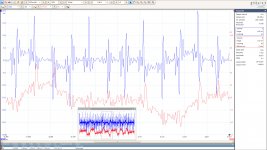
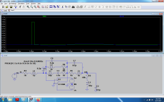
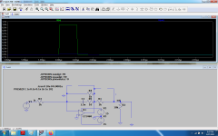
It’s a 5244, 200Mhz, 1.75 nsec risetime, 1Gs/sec 8bits and 0.5Gs/sec 12 bits scope.
I saw no differences in the amplitude or pulse width of the ca 20mV pulses 82nsec apart when sampling at 1Gs/sec@8bits or 0.5Gb/sec@12bits.
I also offered a square wave with a 10nsec risetime wave to check the scopes behaviour. This looked absolutely pristine using the same coax and 50R terminator, no overshoot and no artefacts at this same high sampling rate.
Hans
Syn08,
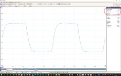
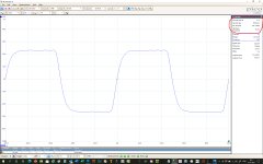
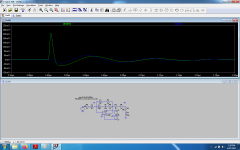
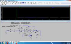
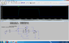
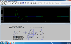
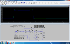
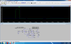
To support my previous posting, here are the recordings of a square wave with a rise time of 9nsec, recorded over the same coax cable and 50R feed-through terminator at resp 1Gs/sec @ 8Bits and 0.5Gs/sec @ 12 bits.
As mentioned, no anomalies and a pristine waveform IMO.
Triggering cannot be much of a problem since my scope stores N recordings with or without triggering, enabling to inspect the frozen recording in all peace.
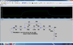
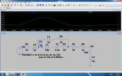
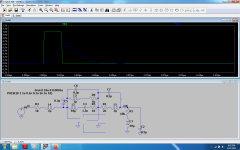
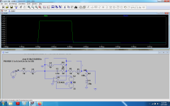
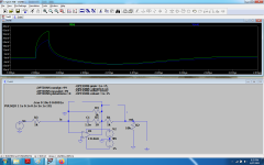
But maybe even more important, the main reason for this exercise was to find out whether the input of a LT1468 voltage feedback amp can get overloaded by those 1mA@2nsec transients from the Dac ?
When looking at the upgoing ramp of a -12dBFs square wave, where successive steps are almost the largest possible ones in audio, wouldn't it lead to something like a "dead" time where the voltage amp has to recover ?
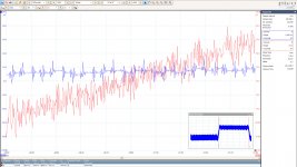
But when looking at the recordings on a 200nsec/div & 20mV/div scale, no such effect is visible, see third image with in blue the voltage from the Dac over 25R and in red the voltage output from the voltage feedback amp, see image nr. 4.
Could the conclusion be drawn in that case that no such amp overload is taking place ?
Hans
To support my previous posting, here are the recordings of a square wave with a rise time of 9nsec, recorded over the same coax cable and 50R feed-through terminator at resp 1Gs/sec @ 8Bits and 0.5Gs/sec @ 12 bits.
As mentioned, no anomalies and a pristine waveform IMO.
Triggering cannot be much of a problem since my scope stores N recordings with or without triggering, enabling to inspect the frozen recording in all peace.
But maybe even more important, the main reason for this exercise was to find out whether the input of a LT1468 voltage feedback amp can get overloaded by those 1mA@2nsec transients from the Dac ?
When looking at the upgoing ramp of a -12dBFs square wave, where successive steps are almost the largest possible ones in audio, wouldn't it lead to something like a "dead" time where the voltage amp has to recover ?
But when looking at the recordings on a 200nsec/div & 20mV/div scale, no such effect is visible, see third image with in blue the voltage from the Dac over 25R and in red the voltage output from the voltage feedback amp, see image nr. 4.
Could the conclusion be drawn in that case that no such amp overload is taking place ?
Hans
Attachments
It's in the grey area, isn't it? The op-amp has a bipolar differential pair input stage, so any error signal >> 2 kT/q ~= 52 mV will drive it into slew rate limiting, any error signal << 2 kT/q will be handled more or less linearly and your 25 mV..40 mV error signal peaks are somewhere in between.
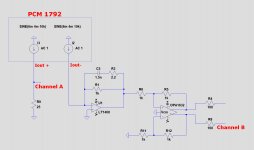
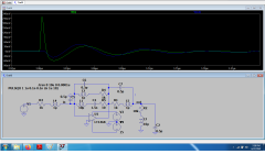
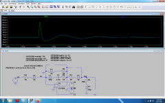
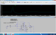
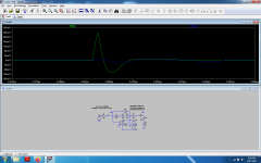
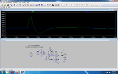
Yes, the circuity diagram is the grey area, image 4 if that is what you are pointing to.
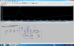
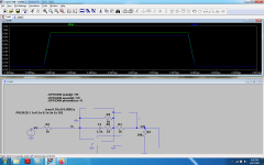
But, we only can see in image 3 that the Dac produces peaks of +/-15 mV at that point, translating into +/-0.6mA, so let's say peaks can be +/- 1mA to stay of the safe side.
What is unknown is the LT1468's Zin, so no idea how this translates into an input voltage and LTSpice is not of any help in this case.
With Zin=2R for these spikes, it would still result in less then the 52mV that you mention, but who knows ?
Putting a probe at the amp's input will probably result in very unreliable results,
so the only thing I could think of was looking if any recovery time from overload was visible at the output, but I don't see that.
Hans
Last edited:
Right, I thought the blue trace of picture 3 showed the error voltage, but it's the voltage across 25 ohm.
The graph at the bottom right of page 7 of the datasheet shows that the output impedance with full feedback varies from 10 ohm at 8 MHz to about 40 ohm above 40 MHz, see https://www.analog.com/media/en/technical-documentation/data-sheets/1468fb.pdf , so the order of magnitude of the peaks should be the same.
The graph at the bottom right of page 7 of the datasheet shows that the output impedance with full feedback varies from 10 ohm at 8 MHz to about 40 ohm above 40 MHz, see https://www.analog.com/media/en/technical-documentation/data-sheets/1468fb.pdf , so the order of magnitude of the peaks should be the same.
Actually that's a bit of a circular reasoning, because the output impedance only applies under small-signal conditions and the question was whether the signal is small...
You are measuring something, but you do not understand how it is.
If the LT1468 works correctly, then why there are such peaks at its exit.
1mA current for 10ns should charge 1,5nF to 0.15mV and we have more.
And here the peak is less than 10ns means in the output should be less than 0.15mV
This peak just goes from the entrance to the output through the condenser and the operational amplifier just does not have time to react.
Last edited:
Hi Sandy,
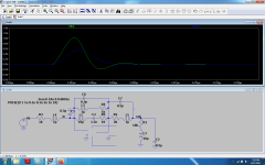
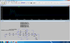
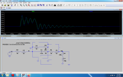
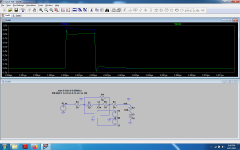
When the current pulses from the Dac are going directly to the amp's output through the feedback capacitor, why then are those voltage excursions shaped so different ?
See magnified image below, in blue the current output pulses and in red the op-amps output.
Hans
P.s. and how does a 1.5nF cap look like for nsec pulses with it’s selfinductance and series resistance ?
.
Attachments
Last edited:
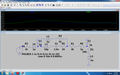
I looked for wima fkp3 1.5nf specs, yet i just had to assume 1u...1mh inductance but 10uh or 1mh give the same results .It seems that the real game changers are the pcb coupling ( probably more than just 1pf ...) and the op-amp itself, but the op-amp is clearly the one affecting the signal the most.The load itself might be inductive by itself and that will work against the op-amp, but not enough. Green signal is the input, blue signal is the output.
Attachments

Last edited:
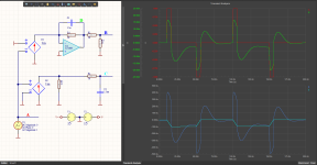
As i forgot to split the 2k resistor when introducing the op-amp....tried that again but obviously the op-amp is still the winner. each resistor will present its own inductance and capacitance at nanosecond signals. You have now the input signal before being transformed into current and what it is seen at the op amp virtual ground .
Attachments
Last edited:
Well...try and measure 1.5nf fkp 3 wima capacitors with 1ma of 2ns signals...i bet you get much higher values than what i used, but you can remove them all and still see that the op-amp is doing most of the attenuation there as the inductances and capacitances of the components aren't doing much by themelves, while the stray capacitance usually found with pcb tracing coupling will muffle the signal with no inductance or higher inducances than what i used....Besides using LTspice medium should give the best sim model for LT1468, right? i could have used .cshunt directive to create stray capacitances everywhere and muffle the signal even more , but this way you can see clearly the results.The passive components by themelves can't reduce the input signal more than 1/3rd of the input energy.It's the op-ap doing the greatest job.Even more, removing completely the inductances you get better results when the op-amp is in, while the usual 0.5pf stray capacitances are pretty low for a real circuit.
Now given the fact that you presented us simulation results pretending they are real measurements, that's disturbing enough for you credibility when atacking other's real measurements and simulations...
Now given the fact that you presented us simulation results pretending they are real measurements, that's disturbing enough for you credibility when atacking other's real measurements and simulations...
Attachments
Last edited:
The first is an old project.
Simulation is on improved designs with reduced noises.
That is exactly what i may try with my 32pieces of pcm63p-y chips. I always wanted to beat krell kav 300cd output stage complexity and here is real chanche to do this with high margin.
I have read whole thread. I really like Sandy.
A lack of sense of humor keeps us upset and not afraid laughing at ourselves keeps us happy and balanced. Simple as it is.
I think I am coolest guy here on all basics man aspects(looks, physical strenght, endurance, health, sucess on womans, libido- you name it), except maybe electronics 😕 Its not my subjective opinion, I rely only on science measurements. 😀
What is really surpsising- how many middle age mans with lot of visceral fats, and low testosterone levels shows bellicosity. that is amazing. 😎
I have never had ability to brag for my achivements until today. If anyone thinks he is tougher guy than my you are welcome in discussion. I did not come here to bring any audio related jewels, just wanted to brag.
and on the seruos note-this is most interesting, valuable forum from all audio forum i have had pleasure to read. keep it up!

You can not use FKP WIMA to filter frequencies> 10-100MHz.
Something like that
Type MLCCs
I just show Hans what to try to measure with this simulation.
Something like that
Type MLCCs
I just show Hans what to try to measure with this simulation.
Last edited:
10 times smaller timestep than the rise/fall time which was already 20 times small than the 2ns impule length so basically 1/200 resolution for the signal plateau, with or without convergence...same sh...t
Attachments


Last edited:
- Home
- Source & Line
- Digital Line Level
- Discrete I-V converter