For the resistors and the caps I would recommend through hole parts. We can get better parts and ones that won't have significant voltage coefficients. All this matters below -120 dB. Possibly the solder mask matters judging from what victor has reported. Maybe hold back the soldermask around the sensitive parts. We should use a nonconductive link between the motor and the pot. Pots are notorious for issues around shaft grounding. if its completely isolated that should not matter (I hope).
There also may be an advantage to adding driven (guard) planes around some of the sensitive circuits to reduce stray capacitances. A resistive divider from a low Z source would be all that is required.
There also may be an advantage to adding driven (guard) planes around some of the sensitive circuits to reduce stray capacitances. A resistive divider from a low Z source would be all that is required.
Thanks a lot for your review.
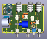
The most critical part is the RC filter (and the pot, of course). Its distortion cannot be compensated. I use a THT resistor there already (the switchable RC filter is the block with 4 capacitors and the THT resistor on the render). The other resistors are SMD to minimize noise pickup now.
My reasoning was the DAC and ADC circuits are full of SMDs and it is the job of the compensation to correct their distortion. Adding a few more SMDs into the to-be-compensated part should not matter.
Distortion outside of the calibration loop cannot be compensated - that being the switchable balanced input attenuator and the by-passable input low-pass filter to reject the bandwidth noise. They are all SMD now too.
I can replace all signal resistors with THT footprints - but would like vertical position for space purposes - is that OK?
Signal capacitors are THT already.
The stepper-pot coupling will be 3D printed, as everything else. I made sure their axes have enough clearance. Actually the stepper and pot holders will be one 3D-printed part to guarantee their axis concentricity.
Regarding the capacity coupling between sections: The 3D-printed enclosure will consist of bottom and top part, internally completely covered with copper tape. The top part will have ribs all the way down to the board at places marked with lines on the board silkscreen. The copper-taped ribs will shield 3 sides of the RC filter (I may add the remaining side to fully enclose the RC filter), and TRS sockets from each other. A rib running across the whole board (along with its mirror on the bottom half of the enclosure) will create two galvanically isolated shielded compartments when the enclosure is closed - for the controlling part and for the signal part. Fully separate grounds, connected to the corresponding shields of each compartment (that is why the board has no solder mask along its edges). The part of the stepper-pot coupling which goes through the shield wall will be narrowed to minimize the non-shielded area.
The pot will be fully taped with copper, so that the voltage-divider path does not interfere with the out-of-phase LPF path. I have this arrangement in my existing adapter and it seems to work OK.
I will avoid the solder mask in the RC filter and other sensitive parts.
Thanks for your help.
Last edited:
For the through hole resistors a .2" spacing should enable most precision resistors as well as 1/4W leaded parts. Personally I would want to minimize nonlinear stuff both inside the correction and outside. Just less to correct.
I was first thinking you would be using one of the Alps motor driven pots but getting the motor to have enough resolution would be an issue. Does the stepper have enough resolution?
I'm feeling way behind the times. I would never have thought of 3D printing parts for something like this.
I was first thinking you would be using one of the Alps motor driven pots but getting the motor to have enough resolution would be an issue. Does the stepper have enough resolution?
I'm feeling way behind the times. I would never have thought of 3D printing parts for something like this.
> DUT terminals:
> * single-ended compensated output
> * balanced input (two BNCs) - hot line compensated, cold line for common-mode rejection of ground loops.
That means no differential output DUTs ?
Or each phase has to be connected to a separate BNC input ?
Patrick
> * single-ended compensated output
> * balanced input (two BNCs) - hot line compensated, cold line for common-mode rejection of ground loops.
That means no differential output DUTs ?
Or each phase has to be connected to a separate BNC input ?
Patrick
Removed the preparation for compensating dual tone by summing two input channels - I think it can be achieved with dual-tone signal from a single channel (to be tested). This simplified the board a bit.
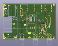
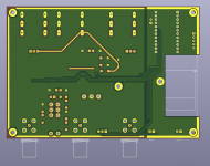
All signal resistors are THT, all signal tracks have solder mask removed (manual chore in kicad 🙂 ).
Rearranged components to allow enclosing both the RC filter and voltage divider into separate shielded compartments.
All signal resistors are THT, all signal tracks have solder mask removed (manual chore in kicad 🙂 ).
Rearranged components to allow enclosing both the RC filter and voltage divider into separate shielded compartments.
Attachments
I was first thinking you would be using one of the Alps motor driven pots but getting the motor to have enough resolution would be an issue. Does the stepper have enough resolution?
These steppers are geared internally. My previous 12V stepper had 18 steps x 1/36 gears = 648 steps per revolution. It took two steps for the multiturn pot to move between neighbouring wire wounds. The final 5V stepper has 32 steps x 1/64 gears = 2048 steps per revolution (times the pot has 10 turns) 🙂 Of course the cheap stepper gears have large play when reversing direction but that is easy to account for in the control feedback loop.
I would never have thought of 3D printing parts for something like this.
I like constructing the whole model in CAD, being able to see all the details on screen first. Then just printing... and one holds the precise materialization of the model in hand.
I want to look at conductive paints for plastic. They are not expensive and would save lots of boring manual work with the copper tape.
>
That means no differential output DUTs ?
Or each phase has to be connected to a separate BNC input ?
Compensating balanced outputs and inputs requires balanced calibration paths - balanced attenuator and balanced LP filter. It may be in the next version of the adapter, but the first make will compensate SE output and SE input only. If a balanced input is available, the on-board jumper can configure the cold line for eliminating ground loop common-mode noise (the second input BNC is then routed to the cold line of the soundcard input). The two BNCs work as balanced input, but calibration is performed with single-ended signal only in the hot line (thus compensating it properly afterwards).
For now I am really interested only in the instantaneous compensation - basically fixing the non-linear gain in DA/AD and in the analog filters of the soundcard. Volterra series are way way above my skills 🙂
I will ask at the library of our local university but doubt they will have this 60 years old US journal. Or I will bite the bullet and cough up those 33 bucks...
Looking at this - it’s very close to back propagation neural networks.
It would be possible to train the network to correct the sound.
It would be possible to train the network to correct the sound.
I think so, especially considering the unlimited amount of training material (just recording long music stream). The recorded track would have to be precisely subsample-shifted to time-fit samples of the original track, but that is a standard operation.
I would be surprised if some researchers had not pursued this path yet, it would have an interesting commercial application. Marketing "Audiophile Artificial Intelligence" could get very creative... 🙂
On the other hand the core of this project is determining the DAC and ADC contributions to the overall loop distortion. Using a neural network for that would be cool too, the DAC-side neural network could pre-distort only the DAC-side contribution, not distortion of the overall loop. But I have no idea how to do that for a general music signal...
Last edited:
The stepper-pot assembly finished in order to finalize position of required holes on the adapter PCB. About 10 stepper steps to reach the adjacent pot wire, 15 steps of backlash, no problem for the control loopback.
Now the PCB can be sent to manufacturing. Meanwhile the assembly mounted onto the existing adapter can be used for writing the stepper support into the compensation software. Things just take time... 🙂
Now the PCB can be sent to manufacturing. Meanwhile the assembly mounted onto the existing adapter can be used for writing the stepper support into the compensation software. Things just take time... 🙂
Attachments

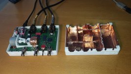
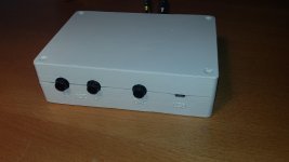
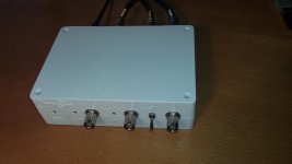
First make of the automated adapter tested and measured. LEDs indicators are still missing, just like input attenuator resistors and the input filter against high-frequency noise (more on that later). Dual LPF filters for (switched at 5kHz) are in place.
Digital (USB ground) and analog (soundcard ground) sections have separate shield compartments.
Taping the copper shield was a boring work, ingredient for the conducting paint are waiting in a box, if I do not decide to shell out the 80 bucks for a 1kg can of non-oxidising nickel conducting paint for plastic. The PCB has no solder mask around the edges on both sides, connecting thus the top/bottom enclosure shields to their corresponding grounds.
The stepper-pot assembly is printed as single piece now to maintain the axis colinear as the stepper running from 5V USB is not particularly strong. ULN2003LVDR low-loss drivers for the stepper feed over 1V more than regular ULN2003 which makes a difference with 5V. In future makes I want to test DRV777s waiting in the box.
Attachments

Automated stepper calibration was interesting to code, it took a few iterations to find a fast-converging algorithm stable at both ends of the range. The code estimates initial pot position and backlash using an equation for position and fitting the parameters with nonlinear regression (I have really learned to appreciate its inherent elimination of real-world measurement deficiencies - noise, random errors, etc.). Often a move of several revolutions (5k+ steps) takes just two iteration cycles (move + subsequent level measurement) to reach level within 0.002dB of the target value.
The software tool implements fully automated (relays + stepper) measurement of the VD and LPF transfers (at all harmonic freqs to the current fundamental), split-sides calibration (optionally looped for permanently calibrated/compensated harmonic generator), and range ADC calibration for the incoming level (at +0.05dB, spot on, -0.05dB below the level) to get interpolation points for slightly fluctuating incoming signal. Every task can be interrupted at any time. When no automated task is running, any relay can be operated from the UI and the stepper (VD) can be ordered to set any level (important for testing).
The software tool implements fully automated (relays + stepper) measurement of the VD and LPF transfers (at all harmonic freqs to the current fundamental), split-sides calibration (optionally looped for permanently calibrated/compensated harmonic generator), and range ADC calibration for the incoming level (at +0.05dB, spot on, -0.05dB below the level) to get interpolation points for slightly fluctuating incoming signal. Every task can be interrupted at any time. When no automated task is running, any relay can be operated from the UI and the stepper (VD) can be ordered to set any level (important for testing).
Attachments

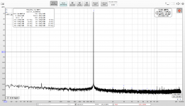
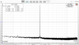
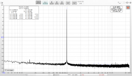
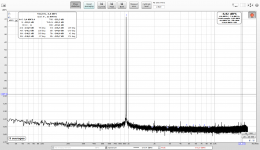
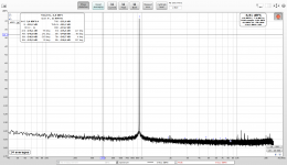
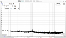
Measurement results, all 128k FFT, 48kHz
1) Split-sides compensation
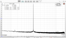
Fig 1 - DAC compensated with split-sides calculation, ADC compensated at VD, switched to VD
Fig2 - results upon flipping the calibration relay to LPF.
I was not sure what a PCB would do with the splitting performance. IMO the construction has not introduced any phase noise and the splitting works decently.
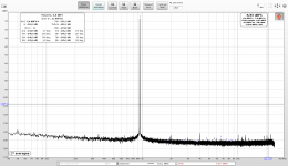
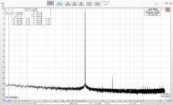
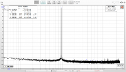
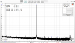
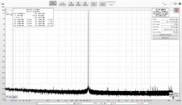
2) VD vs. DUT path distortion
The splitting method just calculates the split. If there is a distortion in the calibration path/s, it will be included in the result. Therefore both paths must be of lowest distortion possible.
I do not have a way to measure the LPF distortion, but brand-new WIMA polyprophylene FKP2 caps are used.
The chinese 10-turn pot was a big question. I tested the distortion with a fixed-resistor attenuator through the external DUT path (can be considered zero distortion for the -130dB THD range of this setup). The VD was set to the same level (+/-0.001dB), joint-sides calibrated, and with the calibration kept running, the path was switched to the fixed attenuator in the DUT loop. While other harmonics did not change, the third one has always crept up a lot. That was a bad sign - if the pot distorts like that, there are not many options to fix it, dead end after all the work.
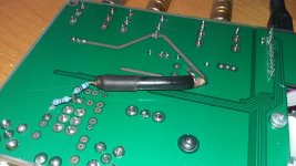
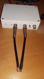
I recalled PMA's test with wide-band noise increasing the 3rd harmonic. I soldered the attenuator directly to the bottom of the board, to avoid output relay contacts, the two BNCs, and the unshielded placement - fig 3.
The results:
Fig 4 - joint-sides calibration through the pot - calibrated for the pot
Fig 5 - switched to the shielded soldered resistor attenuator - compensation kept running.
IMO the pot-path distortion is quite low and the 3rd harmonic present in the external DUT path is really due to BNC contacts/unshielded noise. Next steps will be playing with the input BW filter for which the PCB has preparation and the BNCs which are quite loose (bought locally, quality worse than much cheaper ebay BNCs waiting in the box)
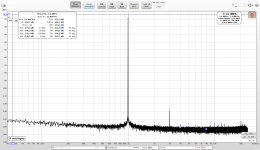
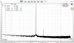
The last figure is base (no compensation) performance of the adapter/soundcard, for comparison.
The setup should be measured in a local university instrumentation&measurement lab in the coming weeks. Well, if the researchers do not fear the Virus, but we dropped our family skiing in italian Dolomites to avoid that..
1) Split-sides compensation
Fig 1 - DAC compensated with split-sides calculation, ADC compensated at VD, switched to VD
Fig2 - results upon flipping the calibration relay to LPF.
I was not sure what a PCB would do with the splitting performance. IMO the construction has not introduced any phase noise and the splitting works decently.
2) VD vs. DUT path distortion
The splitting method just calculates the split. If there is a distortion in the calibration path/s, it will be included in the result. Therefore both paths must be of lowest distortion possible.
I do not have a way to measure the LPF distortion, but brand-new WIMA polyprophylene FKP2 caps are used.
The chinese 10-turn pot was a big question. I tested the distortion with a fixed-resistor attenuator through the external DUT path (can be considered zero distortion for the -130dB THD range of this setup). The VD was set to the same level (+/-0.001dB), joint-sides calibrated, and with the calibration kept running, the path was switched to the fixed attenuator in the DUT loop. While other harmonics did not change, the third one has always crept up a lot. That was a bad sign - if the pot distorts like that, there are not many options to fix it, dead end after all the work.
I recalled PMA's test with wide-band noise increasing the 3rd harmonic. I soldered the attenuator directly to the bottom of the board, to avoid output relay contacts, the two BNCs, and the unshielded placement - fig 3.
The results:
Fig 4 - joint-sides calibration through the pot - calibrated for the pot
Fig 5 - switched to the shielded soldered resistor attenuator - compensation kept running.
IMO the pot-path distortion is quite low and the 3rd harmonic present in the external DUT path is really due to BNC contacts/unshielded noise. Next steps will be playing with the input BW filter for which the PCB has preparation and the BNCs which are quite loose (bought locally, quality worse than much cheaper ebay BNCs waiting in the box)
The last figure is base (no compensation) performance of the adapter/soundcard, for comparison.
The setup should be measured in a local university instrumentation&measurement lab in the coming weeks. Well, if the researchers do not fear the Virus, but we dropped our family skiing in italian Dolomites to avoid that..
Attachments

Last edited:
Thanks Phofman for sharing and a nice device you have made.
Yes drop the skiing, we have a closed country now (Denmark) because of TheVirus....
So time to noodle
Yes drop the skiing, we have a closed country now (Denmark) because of TheVirus....
So time to noodle
The same here (Czech), plus all the beer pubs closed too... 🙂
But I am glad for that, IMO those measures should have been taken earlier, before everyone went and came back from the Alps for the spring vacations... Since I have mostly work in our windowless cellar (a mole workshop), I do not mind the closed everything... My wife being a pro singer is affected more, but kids love the extra vacations ... 🙂
But I am glad for that, IMO those measures should have been taken earlier, before everyone went and came back from the Alps for the spring vacations... Since I have mostly work in our windowless cellar (a mole workshop), I do not mind the closed everything... My wife being a pro singer is affected more, but kids love the extra vacations ... 🙂
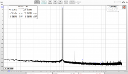
The 3rd harmonic of the Hi-Z (1M) E-MU input changes significantly with source impedance.
Practical example:
The VD pot is 5k. When the DUT path contains attenuator with the same overall resistance of 5k, the compensation works perfectly for calibration path and DUT path
Screenshot 1 - calibration VD path (5k pot) at the same level as DUT path
Screenshot 2 - DUT path - divider 270R + 4k7 - the distortion has not changed
All the following screenshots are for VD-calibration at the corresponding DUT level, that means they describe difference in ADC distortion between source impedance of the pot and that of the DUT divider
Screenshot 3 - divider 680R + 4k7 (slightly more than 5k) - H3 starts rising
Screenshot 4 - divider 390R + 2k7 (60% of VD impedance) - H3 grows a lot
Screenshot 5 - divider 150R + 1k8 (40% of VD impedance) - H3 grows really ugly
Not only is this damaging the ADC-side compensation, but also the calculation of DAC/ADC contributions. VD source impedance and LPF output impedances are different and cannot be easyly aligned without another stepper/pot. That means that ADC distortion profiles for VD path and LPF path are not equal which breaks the necessary condition of the splitting calculation.
OK, how about separating the Hi-Z soundcard input with a unit-gain buffer. OPA1656 in inverting mode takes just two extra resistors (gain 1) + two filtration electrolytes for the +/-12V supply. The buffer easily fits into the adapter enclosure between the last relay and the output socket.
Interestingly, the harmonics structure of the loopback distortion changed quite significantly with the added buffer. I think it is again caused by the changed source impedance seen by the ADC. Since the buffer is in the calibration path, any distortion does not matter, it can be compensated out, of course provided it is not changing.
The result:
Screenshot 6 - VD path compensated, calibrated for VD - that can only be clean
Screenshot 7 - divider 270R + 2k7 - basically no change in distortion profile - compare to screenshot 4 with basically same DUT impedance, but without the buffer.
I think the problem is resolved. OPA1656 buffer is not influenced by the source impedance, while providing constant (very low) source impedance for the actual soundcard input.
Unfortunately the buffer requires a power supply but there are multiple options (supply from the soundcard, from the DAC/ADC frontend which the adapter could be part of, small Lion batteries charged via the USB when not in operation, extra PSU etc.). This is a fun part, once the uncertain stuff works 🙂
The cheap chinese 10-turn pot has basically zero distortion, compared to the hard-soldered voltage divider. Only one relay switch is in both paths (calibration/DUT to the soundcard input). That is an important result too.
BTW it is interesting that the transformer-based power supply creates a minor capacitive ground loop with the switched adapter of the soundcard, causing < -140dB peaks at 1kHz multiples, probably something to do with USB frame frequency. Exactly for this reason do I not use the measurement frequency of 1kHz multiples - 941Hz was used to set the harmonics well apart from the non-related spurious.
Attachments
Last edited:
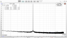
After replacing "gold-plated" almost unsolderable TRS jacks bought from a Central European quite reputable vendor with much cheaper white perfectly solderable jacks from ebay China the H2 stopped playing games and stays rock solid for tens of minutes.
Upon replacing a loose BNC connector and again soldering with special solder paste the almost unsolderable BNCs from another local distributor the initial ugly distortion through the external path with a resistor divider disappeared and these paths are equal now:
Path 1: soundcard output -> adapter TRS -> 10-turn 5k pot -> relay calib/DUT -> OPA1656 -> adapter TRS -> soundcard input. The distortion was joint-sides calibrated/compensated for this path - screenshot 1
Path 2: soundcard output -> adapter TRS -> output relay -> BNC OUT -> external 3k resistor divider -> BNC IN -> white (Ag-plated) toggle switch from chinese ebay -> relay calib/DUT -> OPA1656 -> adapter TRS -> soundcard input. The distortion compensation was calibrated for path 1) - screenshot 2
Clearly the pot path has identical distortion to the relays + BNCs with properly soldered coax and selected for tightness + cheap chinese toggle switch. IME these low THD measurements (all harmonics below -140dBc) are extremely sensitive and every imperfection raises its corresponding harmonics considerably, no room for hiding. IMO the chances of the two paths having larger but absolutely identical distortions (amplitude and phase for all harmonics) in order to achieve the measured no difference are basically zero. Therefore for me the only plausible explanation for the calibration of one path being valid for the second path is that both paths have distortions below measurement error.
Screenshot 3 is external DUT (path 2) with compensation kept running when writing this post - for 20 minutes no change in the harmonics (<-140dBc) of the whole loopback.
Attachments
Last edited:
Very interesting, have you try a linear supply on the EMU & Arduino? To see if it remove the 10-12Khz spikes
Would it not be possible to hack the EMU and add the OPA1656 direct into the A/D input and get rid of the EMU input circuit ?
Would it not be possible to hack the EMU and add the OPA1656 direct into the A/D input and get rid of the EMU input circuit ?
Very interesting, have you try a linear supply on the EMU & Arduino? To see if it remove the 10-12Khz spikes
Arduino power/ground is completely separate, but of course connected to the same PC. E-MU has a switched PSU. I think it is a capacitive ground loop from between the PC and the switched adapter. I flipped the E-MU adapter and the spikes changed - picture 1 vs. 2.
Would it not be possible to hack the EMU and add the OPA1656 direct into the A/D input and get rid of the EMU input circuit ?[/QUOTE]
Actually, I am not so interested in the EMU performance (I have already fixed the known problem with nonsymmetrical routing of left input channel). I need the compensation adapter to work with any decent soundcard. I think the OPA1656 output buffer is universal. But thanks for your help.
Attachments

I changed the +/-12V linear PSU powering the OPA buffer for two 12V/7Ah SLA batteries, to avoid any ground loops.
I returned to measuring my set of opamps. The measurement adapter is powered by the +/-12V SLA batteries too. I removed all the components for distortion multiplier, cleaned the board thoroughly.
Non-inverting voltage follower, noninverting input to ground with 4k7 resistor, output attenuator (to give the VD pot enough room for adjustments) -1dB 1kohm.
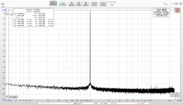
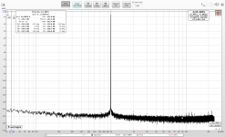
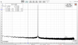
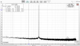
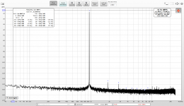
Fig 1 - compensated loopback, this is the calibration etalon. FFT 1M
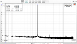
Fig 2 - OPA1656. No difference in THD, the opamp distortion is below < -135dB, below the method precision.
All other measurements are with faster FFT 128k, because at least one harmonic is already clearly above the floor.
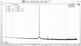
Fig 3 - LM4562 piece 1
Fig 4 - LM4562 piece 2 - both around -128dB. Deeper FFT would should the other harmonics, for FFT 128k only the second was measurable at -130dB
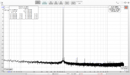
Fig 5 - NE5532 - faring pretty well, -127dB. Unfortunately I have only one piece.
Fig 6 - OPA2132 piece 1
Fig 7 - OPA2132 piece 2 - these are DIP8 versions. 2 pieces of SO8 package measured identically. -126dB
Fig 8 - OP275 piece 1
Fig 9 - OP275 piece 2 - what's wrong with their H2?
I returned to measuring my set of opamps. The measurement adapter is powered by the +/-12V SLA batteries too. I removed all the components for distortion multiplier, cleaned the board thoroughly.
Non-inverting voltage follower, noninverting input to ground with 4k7 resistor, output attenuator (to give the VD pot enough room for adjustments) -1dB 1kohm.
Fig 1 - compensated loopback, this is the calibration etalon. FFT 1M
Fig 2 - OPA1656. No difference in THD, the opamp distortion is below < -135dB, below the method precision.
All other measurements are with faster FFT 128k, because at least one harmonic is already clearly above the floor.
Fig 3 - LM4562 piece 1
Fig 4 - LM4562 piece 2 - both around -128dB. Deeper FFT would should the other harmonics, for FFT 128k only the second was measurable at -130dB
Fig 5 - NE5532 - faring pretty well, -127dB. Unfortunately I have only one piece.
Fig 6 - OPA2132 piece 1
Fig 7 - OPA2132 piece 2 - these are DIP8 versions. 2 pieces of SO8 package measured identically. -126dB
Fig 8 - OP275 piece 1
Fig 9 - OP275 piece 2 - what's wrong with their H2?
Attachments
-
 OP275-1.png124.8 KB · Views: 151
 -
 OPA2132-2.png116.5 KB · Views: 155
 -
 OPA2132-1.png120 KB · Views: 168
 -
 NE5532.png105.6 KB · Views: 231
 -
 LM4562-2.png121 KB · Views: 173
 -
 LM4562-1.png121.6 KB · Views: 195
 -
 OPA1656.png132.3 KB · Views: 207
 -
 VD-calib.png129 KB · Views: 199
 -
 OP275-2.png110.9 KB · Views: 168
Last edited:
- Home
- Design & Build
- Equipment & Tools
- Digital Distortion Compensation for Measurement Setup