Yikes! The memory goes bad when the years creep up. Thanks for the heads-up.
I forgot to remember the darlington arrangement around the ring emitter PNP! This adds two components. However the total voltage drop across R1 (below) is only 1.4V, whereas the voltage drop across R5 in post #95 is 4.0-5.0 volts, thanks to the PMOSFET's large threshold voltage. So the minimum required supply voltage for the all-BJT circuit is about (VREF + 1.7V), while the minimum required supply voltage for the BJT+PMOS is about (VREF + 4.3V).
Also the all-BJT circuit's bandwidth is higher because the really big capacitance is driven by a 25 ohm resistor instead of a 500 ohm resistor. Compare the frequencies at which Zout = 0.003 ohms.
_
Attachments


, whereas the voltage drop across R5 in post #95 is 4.0-5.0 volts, thanks to the PMOSFET's large threshold voltage. So the minimum required supply voltage for the all-BJT circuit is about (VREF + 1.7V), while the minimum required supply voltage for the BJT+PMOS is about (VREF + 4.3V).
_
No no. Read again.
With compound pair it's only Vbe of the bipolar.
THAT'S THE GENIUS PART. Haha
Sorry Mark
Misunderstanding, I was referring to the Voltage drop between base of bipolar and drain of mosfet.
This is where I got overly excited as Vgs would be normally 4 to 5 Volts for a regular mosfet follower, but I now see Vds is still around 4 volts even though the drop from base to drain is only around 0.6V.
Back to being dumb. Hahaha
Anyway, I think I still prefer the bipolar/mosfet in compound pair arrangement.
I'm busy today but I'll be back later.
I might put it all into a word document.
Last edited:
VREF to VOUT is 1xVBE for an emitter follower or for a complementary feedback pair.
HOWEVER VIN to VREF is a more complicated piece of mathematics; and if you use a 500 volt 40 amp MOSFET with standard Vgs threshold voltage, you will discover that VIN to VREF {or if you prefer, VIN to VOUT a/k/a "dropout voltage"} is revolting, awful, and embarrassingly high for the MOSFET option. Do a side by side comparison and then repeat with me, in unison, "Oh Yuck".
HOWEVER VIN to VREF is a more complicated piece of mathematics; and if you use a 500 volt 40 amp MOSFET with standard Vgs threshold voltage, you will discover that VIN to VREF {or if you prefer, VIN to VOUT a/k/a "dropout voltage"} is revolting, awful, and embarrassingly high for the MOSFET option. Do a side by side comparison and then repeat with me, in unison, "Oh Yuck".
Hi Mark
Have you tried MJL4281A/MJL4302A?
Seems to give quite a decent improvement over MJL3281A/MJL1302A
Have you tried MJL4281A/MJL4302A?
Seems to give quite a decent improvement over MJL3281A/MJL1302A
Last edited:
These two sets of transistors are very close.
I suspect the simulation is giving "decent improvement" because the models are very different.
I suspect the simulation is giving "decent improvement" because the models are very different.
compare the models.
Then change the one parameter that has the biggest difference and see if the simulation predictions become similar.
You could gradually work through all the model parameters starting with the biggest differences until the predictions do become identical.
Then change the one parameter that has the biggest difference and see if the simulation predictions become similar.
You could gradually work through all the model parameters starting with the biggest differences until the predictions do become identical.
I have never managed to learn LTspice and I have even less of a clue to how time consumimg and resourse hungry parameter defining becomes. But I believe that R.Cordell has given away, completely free, an enormous data base that many of us here should be eternally grateful.
I take it these are better than snap-ins for your purposes? They probably handle class A heat and ripple current a bit better.
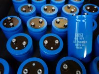
Gonna a build an extreme passive supply first as a reference point for the regulated supplies that will be tested later.
I'm a fan of the cave man approach to electronics. Haha
The big screw terminal caps tend to have much higher ripple current capacity and much lower esr. Also they go to much higher capacitance levels than snap-ins. The ones I purchased are 220,000uF each.
I'm a fan of the cave man approach to electronics. Haha
The big screw terminal caps tend to have much higher ripple current capacity and much lower esr. Also they go to much higher capacitance levels than snap-ins. The ones I purchased are 220,000uF each.
Last edited:

- Home
- Amplifiers
- Pass Labs
- Developing a Regulated Dual Rail Power Supply For FirstWatt Amps