the last topology
Alaskan audio 1R1 power amp : http://lanouettetech.com/Projets/AudioAmp/AlaskaanPwrAmp/9500102a.pdf
Hi Rikard,
I'm not sure whether adding extra caps will really help, because of:
1- extra loading of the drivers.
2- the absolute values of the nonlinearities are still the same.
I'm not sure whether adding extra caps will really help, because of:
1- extra loading of the drivers.
2- the absolute values of the nonlinearities are still the same.
Alaskan audio 1R1 power amp : http://lanouettetech.com/Projets/AudioAmp/AlaskaanPwrAmp/9500102a.pdf
Hi Jacco,
Interesting amp and .... separate push-pull drivers. 🙂
According to Mr Cordell the Toshibas are vertical, or at least behaves like verticals. I can confirm they do have a slightly positive temp coeff up to several amps bias. Besides, measuring the top output current at about 40 amps into a 1 ohm load (prototype) would suggest they are not lateral, right?
On the other hand, I found them less prone to oscillation than th IRFPs which are used in this sim. I´ll try to check the slewrate in real life for the prototype which has Toshiba´s in it.
I simmed it with 10 nF, 100 nF and 2,2 uF parallell to the load. Pics attached.
🙂
Hi Rickard,
You are correct; they are verticals. Although they have lower Vgs_on than the IR Hexfet devices, they should not be confused with Laterals.
Cheers,
Bob
this is from the toshiba data book. "pi"-MOS is lateral, u-Mos is vertical
Hi Unclejed,
DMOS, as described under piMOS is considered a conventional vertical MOSFET.
The other diagram refers to a newer generation of vertical MOSFETs called TrenchFETs. They are a type of vertical MOSFET that is characterized by extremely low ON resistance.
I have never used TrenchFETs in a linear audio amplifier, and believe that I have read that they are generally not a good choice for linear applications.
Cheers,
Bob
201/1530
just read the pin out to confirm they are not Lfets.Of course they are vertical MOSFETs, what else? Period.
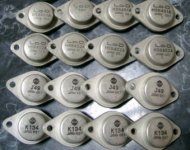
Toshiba Fets
Have looked several times at using these DMOS parts. 2SK1530/2SJ201. and the lower power 2SK1529/2SJ200.
Unfortunately the 'O' grade devices (with the lower Vgs th/off - almost lateral like) do not seem to be readily available. The 'Y' grades are. This to me is what makes them good plus better complimentary matching over IRFs.
I suspect you get lower crossover distortion with 'O' grade over the 'Y' grades. And less headroom is needed - not that I am worried about that. I may be wrong but the 'Y' grades do not really justify paying more (seen them for £8 a piece in UK) than standard IRF parts.
Anyone compared them audibly in amp output stages ?
Do lower Vgs(off) parts have lower crossover distortion (all things being equal) ?
Fanuc,
Lower Vgs threshold voltage always means greater linearity. Crossover distortion is a more complex matter.Do lower Vgs(off) parts have lower crossover distortion (all things being equal) ?
Lower Vgs threshold voltage always means greater linearity.
As usual, 100% incorrect. There is no correlation between the threshold voltage and linearity, unless you have your own definition of "linearity".
syn08,
unconditionally correct. I considerately gave you the conducive advice to check your sources carefully and stop filling this otherwise great site with unwarrantable and unfounded claims.
unconditionally correct. I considerately gave you the conducive advice to check your sources carefully and stop filling this otherwise great site with unwarrantable and unfounded claims.
syn08,
unconditionally correct. I considerately gave you the conducive advice to check your sources carefully and stop filling this otherwise great site with unwarrantable and unfounded claims.
Hi Lumba,
I also am unaware of any general correlation between threshold voltage and linearity. So I have to agree with syno8. If you have a credible reference that shows that DMOS MOSFETs with lower threshold voltage have higher linearity I would like to see it.
It is also very important that individual device linearity characteristics not be confused with the amount of crossover distortion likely to be generated in a class AB output stage. The crossover distortion is often dominated by transconductance droop and transconductance mismatch in the crossover region.
For a given amount of bias current, you tend to want more transconductance, so as to minimize transconductance droop. One thing to look at is the transconductance at 150 mA. You would also like that transconductance to be as much the same as possible for the N and P devices.
Cheers,
Bob
It is also very important that individual device linearity characteristics not be confused with the amount of crossover distortion likely to be generated in a class AB output stage. The crossover distortion is often dominated by transconductance droop and transconductance mismatch in the crossover region.
For a given amount of bias current, you tend to want more transconductance, so as to minimize transconductance droop. One thing to look at is the transconductance at 150 mA. You would also like that transconductance to be as much the same as possible for the N and P devices.
This is a very good description. I guess what you mean by "transconductance mismatch in the crossover region" is actually the subthreshold (exponential) mismatch. This mechanism (actually the subthreshold conduction slope gap to the theoretical 60mV/decade) is of course independent to the threshold voltage value as well.
Hi Bob,
you should better agree with me.
I`m was talking about Vgs linearity, but the same applies to Vbe, which is a main cause of nonlinearity: reducing it improves the poor Vbe/Ic functional relationship.
It is desirable to have a flat transconductance gain characteristic, obtained at low gate voltages and over a wide range of gate voltage.
It should be obvious to almost everyone that it is harder to achieve flat characteristics over a wider range. A smaller excursion range does mean better linearity. Source degeneration helps, since part of the input signal drops on the resistance, thus for the same amplitude (and power), Vgs is reduced, thereby the distortion. (Generally, this is the simplest, but a very efficient linearization technique). At high overdrive voltages, however, it may result in an unadvantageous Gm attenuation and may also have other disadvantages.
The lower Vt is an important reason for the superiority of lateral MOSFETs, although far from the only one. Channel geometry and length is another reason. Hitachi`s lateral MOSFET die design is thirty five years old, but highly likely formed the base for the most linear power semiconductor devices ever made. In the mean time the vertical (double diffused MOS) technology has been prominently developed, allowing shorter (T-shaped) channel lengths. The trouble is that short channels are stubborn and hard to control, it occurs much more accurately in the tight lateral structure.
A relevant equation:
Id=WCo(Vg-Vt)vs
W=channel width
Co=gate oxide capacitance
Vg=applied gate voltage
Vt=gate threshold voltage¤
(Vg-Vt)=Vod=overdrive voltage
vs=electron drift velocity
¤Voltage causing 1uA to flow, not quite the same as Vgs(th) in data sheets, which is measured at high drain currents.
Linearity is a tricky matter at high currents, where the Vod/Id proportionality deteriorates considerably. Besides, several parameters decisive for linearity are strongly temperature dependent.
Hi Bob,
you should better agree with me.
I`m was talking about Vgs linearity, but the same applies to Vbe, which is a main cause of nonlinearity: reducing it improves the poor Vbe/Ic functional relationship.
It is desirable to have a flat transconductance gain characteristic, obtained at low gate voltages and over a wide range of gate voltage.
It should be obvious to almost everyone that it is harder to achieve flat characteristics over a wider range. A smaller excursion range does mean better linearity. Source degeneration helps, since part of the input signal drops on the resistance, thus for the same amplitude (and power), Vgs is reduced, thereby the distortion. (Generally, this is the simplest, but a very efficient linearization technique). At high overdrive voltages, however, it may result in an unadvantageous Gm attenuation and may also have other disadvantages.
The lower Vt is an important reason for the superiority of lateral MOSFETs, although far from the only one. Channel geometry and length is another reason. Hitachi`s lateral MOSFET die design is thirty five years old, but highly likely formed the base for the most linear power semiconductor devices ever made. In the mean time the vertical (double diffused MOS) technology has been prominently developed, allowing shorter (T-shaped) channel lengths. The trouble is that short channels are stubborn and hard to control, it occurs much more accurately in the tight lateral structure.
A relevant equation:
Id=WCo(Vg-Vt)vs
W=channel width
Co=gate oxide capacitance
Vg=applied gate voltage
Vt=gate threshold voltage¤
(Vg-Vt)=Vod=overdrive voltage
vs=electron drift velocity
¤Voltage causing 1uA to flow, not quite the same as Vgs(th) in data sheets, which is measured at high drain currents.
Linearity is a tricky matter at high currents, where the Vod/Id proportionality deteriorates considerably. Besides, several parameters decisive for linearity are strongly temperature dependent.
Your equation is wrong. It is misleading to use here the drift velocity, since it depends in turn on (Vg-Vt), following vs=Us*E and E~1/(Vg-Vd) It resembles a little (also missing the -Vds^2/2 term) the current equation in triode (linear) region Vds < Vgs-Vt, which is totally irrelevant for a MOSFET amplifier, always working in the saturation region. Correct is (using your notations):
Id=(1/2)*(W/L)*Us*Co*(1+Lambda*Vds)*(Vg-Vt)^2
Hence the transconductance:
Gm=(W/L)*Us*Co*(Vg-Vt)
where Us is the majority carrier mobility, and L is the channel legth. The above equation are written in the hypothesis that there are no longitudinal field effects, that is, Vds is small and Lambda is negligible.
There isn't anything like "Vgs linearity". The rest of your "explanation" is gibberish.
You may want to consider the Gm linearity. The factors affecting linearity are (in a first approximation):
- carrier mobility saturation/degradation at high injection levels (accounting fro the "Gm droop").
- Lambda, the channel modulation coefficient, modulating the drain current with Vds.
- Subthreshold conduction (not captured in the above equations) where the diffusion conduction mechanism dominates; the MOSFET behaves essentially as a BJT, having an exponential dependency of the drain current on Vgs. For MOSFET power devices, the subthreshold region may extend well into the mA and 10's of mA. This is one of the reasons why MOSFET power stages require more bias current than bipolars, for the same distortion performance.
None of the above mechanisms depend on the threshold voltage. Your bed time story about lateral MOSFETs is nothing but another laughable audio myth. BTW, there are vertical MOSFETs with low threshold voltage available.
syn08,
the classic square wave equation does not hold for high currents, short channels and strong electric fields. Forget about it.
the classic square wave equation does not hold for high currents, short channels and strong electric fields. Forget about it.
Not many. I´m only aware of these from Toshiba. That`s why they are more linear.BTW, there are vertical MOSFETs with low threshold voltage available.
syn08,
the classic square wave equation does not hold for high currents, short channels and strong electric fields. Forget about it.
Not many. I´m only aware of these from Toshiba. That`s why they are more linear.
Everything is modelled by the equations I gave; high current by mobility degradation, short channels and strong electric field by Lambda. The very short channel MOSFETs are a different kettle of fish and have nothing to do with audio and power devices.
Check the Logic Level devices from Fairchild.
The threshold voltage value has absolutely nothing to do with the device linearity, period. Please stop perpetrating nonsense.
Hitachi`s lateral MOSFET die design is thirty five years old
For the sake of historical accuracy.
Originals at the top, the HS8401 and HS8402 were manufactured in A, B, and C versions.
The first Lateral Mosfet power amplifiers are from the late 1970s : Lo-D/Dynaharmony.
Hitachi issued a piece of paper in 1984, but the technology was older.
Attachments
- Status
- Not open for further replies.
- Home
- Amplifiers
- Solid State
- Designing amp with 2SJ201/2SK1530