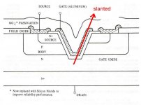
toshiba lists them as pi-MOS, as opposed to u-MOS. toshiba's FET data book shows pi-MOS as lateral device construction, and u-MOS as vertical construction.
unclejed613,
they are (somewhat peculiar) verticals, mainly having the characteristics of vertical structure, although Toshiba has never announced a closer description, as far as I know.
they are (somewhat peculiar) verticals, mainly having the characteristics of vertical structure, although Toshiba has never announced a closer description, as far as I know.
According to Mr Cordell the Toshibas are vertical, or at least behaves like verticals. I can confirm they do have a slightly positive temp coeff up to several amps bias. Besides, measuring the top output current at about 40 amps into a 1 ohm load (prototype) would suggest they are not lateral, right?
On the other hand, I found them less prone to oscillation than th IRFPs which are used in this sim. I´ll try to check the slewrate in real life for the prototype which has Toshiba´s in it.
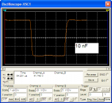
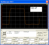
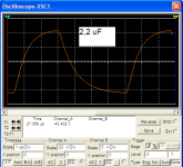
I simmed it with 10 nF, 100 nF and 2,2 uF parallell to the load. Pics attached.
🙂
On the other hand, I found them less prone to oscillation than th IRFPs which are used in this sim. I´ll try to check the slewrate in real life for the prototype which has Toshiba´s in it.
I simmed it with 10 nF, 100 nF and 2,2 uF parallell to the load. Pics attached.
🙂
Attachments

I'm jumping in a bit late, haven't read the entire thread -- but would commend to the community Troy Huebbner's application note AN-1645 on National's website -- the 2SJ201/K1530 were used with the LM4702 -- there's a comprehensive survey of other MOSFETs used with this driver chip: http://www.national.com/an/AN/AN-1645.pdf

jackinnj,
it´s worth reading.
The high rail voltages make choosing a favorable bias current level difficult here.
it´s worth reading.
The high rail voltages make choosing a favorable bias current level difficult here.
I'm jumping in a bit late, haven't read the entire thread -- but would commend to the community Troy Huebbner's application note AN-1645 on National's website -- the 2SJ201/K1530 were used with the LM4702 -- there's a comprehensive survey of other MOSFETs used with this driver chip: http://www.national.com/an/AN/AN-1645.pdf
Hi jackinnj,
Thx for the link. Also notice the different values of the gate stoppers for the 2SJ201/2SK1530 pair: 175 resp. 500 Ohms.
Regards,
Edmond.
Great article! Interestingly the best results were obtained using the Toshiba FETs, which produced the lowest distorsion and the highest slewrate when driven from a proper driver. I guess I made the right choice then. 🙂
About the gate resistors, I´m a bit surprised their optimum values differ so much between N- and P-channel. I will do som more sims and see if it matters. Wish I had the SPICE models for J201/K1530.....
About the gate resistors, I´m a bit surprised their optimum values differ so much between N- and P-channel. I will do som more sims and see if it matters. Wish I had the SPICE models for J201/K1530.....
Hi Rikard,
As for gate resistors see: http://www.diyaudio.com/forums/soli...terview-error-correction-276.html#post1354735
As for gate resistors see: http://www.diyaudio.com/forums/soli...terview-error-correction-276.html#post1354735
this is from the toshiba data book. "pi"-MOS is lateral, u-Mos is vertical
According to the pictures, both pi- and u- are vertical MOSFETs. Here's the lateral MOSFET and a brief comparison:
http://www.fairchildsemi.com/an/AN/AN-558.pdf
The diagrams are conceptual only, but you would of course note the lateral P type substrate (actually connected electrically to the N source) and the vertical N type substrate, electrically the drain. Which also explains the different pinouts of lateral and vertical devices. The center pin is always connected to the substrate and is the source for laterals and the drain for verticals.
So what would you say is better, using different gate resistors or adding extra capacitance for the N-channel gate and keep the equal resistors?
gate resistors; drivers
Although equalizing the capacitances of both genders has appeal in its own right, it's hard to get capacitors with the same nonlinear properties as the internal Cgd and Cgs.
So let's keep it simple, i.e. using different gate resistors.
How about the drivers? There exist three main topologies:
1- One NPN tranny driving the N-Channel MOSFET(s) and one PNP tranny driving the P-channel counterpart(s).
2- One PNP tranny driving the N-Channel MOSFET(s) and one NPN tranny driving the P-channel counterpart(s), plus two additional current sources connected to the emitters of the drivers. See YAP as an example.
3- Each MOSFET gender has its own push-pull PNP/NPN driver.
Opposed to the last topology, notice that the first two topologies need also a cross coupled capacitor between the emitters (of the drivers). It's this capacitor that disturbs the bias setting if the amp is subjected to a 20kHz square wave or whatever nasty signal. In case #1 this cap gets overcharged, thus increasing the bias.
In case #2 this cap gets 'undercharged', thus decreasing the bias.
Omitting this evil cap is no option either, as it will have a devastating effect on the turn-off respectively turn-on times of the MOSFETs.
Therefore, I prefer topology #3 as no cap is needed at all (and if present it will not getting over- or undercharged). Moreover, in case of multiple MOSFETs pairs, you need quite a lot of driving power, so using four driver trannies isn't that much of an overkill anyhow.
BTW, in terms of needed silicon it makes no difference at all. In case #1 or #2 you need two 'big' drivers, while in case #3 you need four trannies of only half the size, as the currents are spread over four devices instead of two.
Comments invited.
Thanks for your answer! The topology is finished, you might want to download the ms8-file a few posts ago. I figured that since the gate capacitances are nonlinear, we might improve matters by adding extra capacitance in parallell. This way, the total capacitance would be less nonlinear, right?
- Status
- Not open for further replies.
- Home
- Amplifiers
- Solid State
- Designing amp with 2SJ201/2SK1530