Have a look at the VFET "output stage" circuit design, attached to post #55 in this thread. It's got some protection mechanisms against terrible input. See whether you think those protections are inadequate for HV "front end" circuits.
You forgot one requirement; no HV circuit failure can wreck the VFET. I get the feeling that there are no more available... 🙂
Have a look at the VFET "output stage" circuit design, attached to post #55 in this thread. It's got some protection mechanisms against terrible input. See whether you think those protections are inadequate for HV "front end" circuits.
Very good points. Added this to the list of design targets. I'd say a good DC blocking capacitor in the output of the front end should do it. If you look carefully, the VFET amp already has a DC blocker. We just need to be sure this cap will withstand the B+ voltage of the front end board.
Why do you want to swing 2V peak? That would mean 17V rms out.
I don't see how your math works. 2 Vpk x 7.5 gain = 15 Vpk = 10.6 Vrms(sine) at the output of the front end. Given the voltage loss across the output stage, this will end up well below 10 Vrms at the amplifier output. Just take a look at the corresponding posts further up this thread.
However the 3V4 has other disadvantages....you need a ... a dedicated filament supply. At this point I would consider using a proper transformer which would not be too big or heavy. A good Antek toroidal or R-core of suitable rating will be good.
To cover the dropout of the CCS / gyrator plus the pk-pk voltage swing, seems that 36V rail would need a boost. Using a dedicated B+ supply would open up a world of possibilities.
Sure. However, we want to run the B+ supply off the 36 VDC in the amp. There is no AC, so a good old transformer will not work. Again, please take a look at the corresponding posts further up the thread.
The filament supply for the 3V4 tube (2.8 V / 50 mA) would be super easy to implement by a simple 660 Ohm dropping resistor from the 36 VDC supply.
Last edited:
How about a low mu triode loaded by a gyrator / hybrid mu-follower, à la Ale Moglia's 01A preamp? Low distortion, low output impedance buffered by the lower gyrator device, JFET in Ale's case.
That's what I'm working on but with 2P29L tubes
2P29L DHT Preamp – Bartola(R) Valves
I embarked on this build as a front end for a MoFo - it will have its own chassis so that it might be deloyed in other use cases, such as with the lottery VFET amp, Ben Mah's follower, etc.
IMO, the thinking around designing a tube front end that will fit into the beautiful VFET chassis is flawed and could result in too many compromises just to squeeze it in without hacking the chassis - the VFET chassis has phono input sockets on its rear panel so build an external front end and run the VFET just with its output stage and free up the options for the front end.
If people really want to try and shoehorn a tube front end in to the VFET it might be worth a look at the various Russian sub-miniature tubes, for example;
http://www.vanderheem.info/Russian_Subminiature-Tubes.pdf
Last edited:
Nelson Pass said the OS H2 is positive phase, but I simply can not understand how. Perhaps it is better to have a measurement confirmation before proceeding to avoid wrong design effort.Ok, need to be more specific about the design targets: The front end should be low-distortion. 2nd harmonic in opposite phase than that of the output stage would be preferred...
Nelson Pass said the OS H2 is positive phase, b.
HI start here https://www.firstwatt.com/pdf/art_h2_v1.pdf
you will find a lot more article
The gain depends quite substantially on the load until the load value is several times the internal resistance. At that point the gain will be closer and closer to mu of the tube. You can draw the loadline on the curves for 1M effective load. Bias point 36V/28uA at -0.5V bias. For each 1V peak you get 12V peak output. So the gain is 12x.I don't see how your math works. 2 Vpk x 7.5 gain = 15 Vpk = 10.6 Vrms(sine) at the output of the front end. Given the voltage loss across the output stage, this will end up well below 10 Vrms at the amplifier output. Just take a look at the corresponding posts further up this thread.
The filament supply for the 3V4 tube (2.8 V / 50 mA) would be super easy to implement by a simple 660 Ohm dropping resistor from the 36 VDC supply.
You can run the 3V4 with the 2 internal filaments in series for 2.8V/50mA but performance is better with filaments in parallel and running at 1.4V/100mA.
And of course, if those curves are related to 1 plate and 1 grid operating, when the 2 grids are tied together and so the 2 plates the anode current will double, the mutual conductance will double and the plate resistance with be halved. So the same result will be obtained for 0.5M load. But 1M would still be desirable to improve distortion figures. The change in gain will not be a lot but still increasing a bit....
A source follower P-channel square law device loaded by a current source should give negative phase H2. How does the 2SJ28 follower create positive phase H2 at 18V and 1.6A bias?HI start here ...
The 2SJ28 follower is not a square law device, it's a VFET. The second sentence in Nelson Pass's VFET design document says "These are special field effect transistors with a characteristic similar to Triode tubes".
AFAIK, all FETs be it Jfet, SIT, VFET or MOSFET including both depletion and enhancement is square law device, easily seen from Id vs Vgs curves. But yes, Vds vs Id curve set for SIT (or VFET) is triodish.
Last edited:
My personal preference would be to try and work with the rail voltages that are present ( and to keep it friendly to someone not accustomed to HV )
A tube optimized for field work such as the ECC86/6GM8 will probably work well with these voltages.
http://www.r-type.org/pdfs/ecc86.pdf
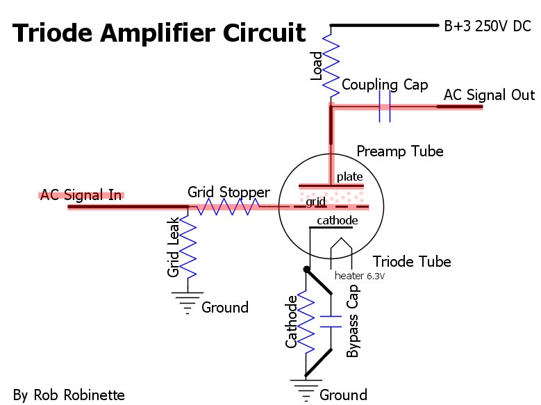
A simple triode gain stage
and use a buck regulator to drop the rail voltages to 6.3V for the heaters

A tube optimized for field work such as the ECC86/6GM8 will probably work well with these voltages.
http://www.r-type.org/pdfs/ecc86.pdf
A simple triode gain stage
and use a buck regulator to drop the rail voltages to 6.3V for the heaters
A tube optimized for field work such as the ECC86/6GM8 will probably work well with these voltages.
I already looked at the ECC86. Unfortunately the curves show that it will be difficult to bias the ECC86 with the grid at -2 V or lower in order to allow the input signal to swing +/- 2 V.
ERRATA CORRIGE: I have just realized I made a mistake about the bias point...32V/28uA with a bias of +1V....the result is fine: with 1M load 1V input gives 12V out.
...assumes the capacitance of the SIT/VFET gate is negligible. Is it? I'll try to do a measurement using the SITs I have at hand.
I biased a 2SJ28 to 1.4A / 22V with a 4 Ohm dummy load. The gate was driven from a sine generator via a DC blocking cap and a 1 kOhm gate stopper resistor. I started at 1 kHz and increased the frequency until the output dropped to 50%, which was at 1.45 MHz. If my math is right, the gate capacitance is about 100 pF or less. It should be a relatively easy load to drive.
All you need to do is ensure the source follower driving the VFET stage has enough current to cope with the capacitance. Set the capacitance at 150 pF, just to be on the safe side, and see what current is needed to drive the VFET cleanly up to a given frequency.
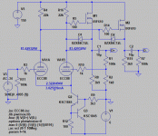
How about an ECC88 cathode coupled amplifier?
Predicted THD <0.013% and H2/H3 > 20dB.
Predicted THD <0.013% and H2/H3 > 20dB.
Code:
Fourier components of V(d+)
DC component:-3.88492e-006

Harmonic	Frequency	 Fourier 	Normalized	 Phase  	Normalized
 Number 	  [Hz]   	Component	 Component	[degree]	Phase [deg]
    1   	1.000e+03	4.000e+00	1.000e+00	   -0.05°	    0.00°
    2   	2.000e+03	5.136e-04	1.284e-04	  -89.90°	  -89.85°
    3   	3.000e+03	2.831e-05	7.078e-06	    1.71°	    1.76°
    4   	4.000e+03	2.099e-07	5.247e-08	   89.73°	   89.79°
    5   	5.000e+03	1.602e-08	4.006e-09	 -174.48°	 -174.43°
    6   	6.000e+03	1.627e-09	4.068e-10	   -8.50°	   -8.45°
    7   	7.000e+03	7.060e-10	1.765e-10	 -162.82°	 -162.76°
    8   	8.000e+03	1.035e-09	2.588e-10	  144.67°	  144.73°
    9   	9.000e+03	2.095e-09	5.237e-10	  113.19°	  113.24°
Total Harmonic Distortion: 0.012861%(0.012860%)

Fourier components of V(d-)
DC component:4.66173e-005

Harmonic	Frequency	 Fourier 	Normalized	 Phase  	Normalized
 Number 	  [Hz]   	Component	 Component	[degree]	Phase [deg]
    1   	1.000e+03	4.001e+00	1.000e+00	  179.95°	    0.00°
    2   	2.000e+03	4.821e-04	1.205e-04	   89.66°	  -90.28°
    3   	3.000e+03	2.832e-05	7.078e-06	 -178.30°	 -358.25°
    4   	4.000e+03	2.044e-07	5.109e-08	  -89.64°	 -269.59°
    5   	5.000e+03	1.854e-08	4.635e-09	    3.92°	 -176.03°
    6   	6.000e+03	4.358e-09	1.089e-09	   -2.04°	 -181.99°
    7   	7.000e+03	1.116e-09	2.788e-10	  -62.96°	 -242.91°
    8   	8.000e+03	1.549e-09	3.873e-10	  -40.49°	 -220.44°
    9   	9.000e+03	1.912e-09	4.780e-10	  -17.39°	 -197.34°
Total Harmonic Distortion: 0.012070%(0.012070%)
Attachments


Hmm, input signal is -9.4 dBv with respect to GND (Figure 1), and D+ output signal is +10.2 dBv with respect to GND (Figure 2).
So gain is (10.2 - (-9.4)) = 19.6 dB to the D+ pin: 9.55 volts per volt . Presumably gain to the D- pin is equal and opposite: -9.55 volts per volt. Total gain is thus 19.1 volts per volt.
That doesn't seem compatible with a max input signal level of 3V RMS.
_
So gain is (10.2 - (-9.4)) = 19.6 dB to the D+ pin: 9.55 volts per volt . Presumably gain to the D- pin is equal and opposite: -9.55 volts per volt. Total gain is thus 19.1 volts per volt.
That doesn't seem compatible with a max input signal level of 3V RMS.
_
Last edited:
- Home
- Amplifiers
- Tubes / Valves
- Designing a vacuum tube front end card for the VFET DIY amp